SBAS710A September 2016 – June 2017 ADS9120
PRODUCTION DATA.
- 1 Features
- 2 Applications
- 3 Description
- 4 Revision History
- 5 Pin Configuration and Functions
-
6 Specifications
- 6.1 Absolute Maximum Ratings
- 6.2 ESD Ratings
- 6.3 Recommended Operating Conditions
- 6.4 Thermal Information
- 6.5 Electrical Characteristics
- 6.6 Timing Requirements: Conversion Cycle
- 6.7 Timing Requirements: Asynchronous Reset, NAP, and PD
- 6.8 Timing Requirements: SPI-Compatible Serial Interface
- 6.9 Timing Requirements: Source-Synchronous Serial Interface (External Clock)
- 6.10 Timing Requirements: Source-Synchronous Serial Interface (Internal Clock)
- 6.11 Typical Characteristics
-
7 Detailed Description
- 7.1 Overview
- 7.2 Functional Block Diagram
- 7.3 Feature Description
- 7.4 Device Functional Modes
- 7.5
Programming
- 7.5.1 Data Transfer Frame
- 7.5.2 Interleaving Conversion Cycles and Data Transfer Frames
- 7.5.3 Data Transfer Protocols
- 7.5.4 Device Setup
- 7.6 Register Maps
- 8 Application and Implementation
- 9 Power-Supply Recommendations
- 10Layout
- 11Device and Documentation Support
- 12Mechanical, Packaging, and Orderable Information
Package Options
Mechanical Data (Package|Pins)
- RGE|24
Thermal pad, mechanical data (Package|Pins)
- RGE|24
Orderable Information
1 Features
- Sample Rate: 2.5 MSPS
- No Latency Output
- Excellent DC and AC Performance:
- INL: ±0.25 LSB
- DNL: ±0.6 LSB
- SNR: 96 dB, THD: –118 dB
- Wide Input Range:
- Unipolar Differential Input Range: ±VREF
- VREF Input Range: 2.5 V to 5 V,
Independent of AVDD
- Low-Power Dissipation:
- 9 mW at 2.5 MSPS (AVDD Only)
- 15.5 mW at 2.5 MSPS (Total)
- Flexible Low-Power Modes Enable Power Scaling with Throughput
- Enhanced-SPI (multiSPI™) Digital Interface
- JESD8-7A-Compliant Digital I/O at 1.8-V DVDD
- Fully-Specified Over Extended Temperature Range: –40°C to +125°C
- Small Footprint: 4-mm × 4-mm VQFN
2 Applications
- Test and Measurement
- Motor Control
- Medical Imaging
- High-Precision, High-Speed Industrial
3 Description
The ADS9120 is a 16-bit, 2.5-MSPS, successive approximation register (SAR) analog-to-digital converter (ADC) with enhanced performance features. The high throughput enables developers to oversample the input signal to improve dynamic range and accuracy of the measurement. The ADS9110 is a pin-compatible, 18-bit, 2-MSPS variant of the ADS9120.
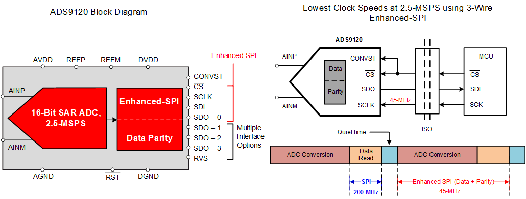
The ADS9120 boosts analog performance while maintaining high-resolution data transfer by using TI’s enhanced SPI feature. Enhanced SPI enables the ADS9120 to achieve high throughput at lower clock speeds, thereby simplifying board layout and lowering system cost.
Enhanced SPI also simplifies the host clocking-in of data, thereby making the device ideal for applications involving FPGAs and DSPs. The ADS9120 is compatible with a standard SPI Interface. The ADS9120 has an internal data parity feature that can be appended to the ADC data output. ADC data validation by the host, using parity bits, improves system reliability.
The device supports JESD8-7A compliant I/Os, the extended industrial temperature range, and is offered in a space-saving, 4-mm × 4-mm, VQFN package.
SPI Interface Clock at Full Throughput(1)
| PART NUMBER | 3-WIRE SPI | 3-WIRE ENHANCED-SPI |
|---|---|---|
| ADS9120 | 200 MHz | 45 MHz |
- For all features of the enhanced SPI, see the Interface Module section.
Ease of System Design with ADS9120
