SBAS876C August 2018 – June 2019 ADS9224R , ADS9234R
PRODUCTION DATA.
- 1 Features
- 2 Applications
- 3 Description
- 4 Revision History
- 5 Pin Configuration and Functions
-
6 Specifications
- 6.1 Absolute Maximum Ratings
- 6.2 ESD Ratings
- 6.3 Recommended Operating Conditions
- 6.4 Thermal Information
- 6.5 Electrical Characteristics: ADS92x4R
- 6.6 Electrical Characteristics: ADS9224R
- 6.7 Electrical Characteristics: ADS9234R
- 6.8 Timing Requirements
- 6.9 Switching Characteristics
- 6.10 Typical Characteristics: ADS9224R
- 6.11 Typical Characteristics: ADS9234R
-
7 Detailed Description
- 7.1 Overview
- 7.2 Functional Block Diagram
- 7.3 Feature Description
- 7.4 Device Functional Modes
- 7.5 READY/STROBE Output
- 7.6
Programming
- 7.6.1 Output Data Word
- 7.6.2
Data Transfer Protocols
- 7.6.2.1
Protocols for Reading From the Device
- 7.6.2.1.1 Legacy, SPI-Compatible Protocols (SPI-xy-S-SDR)
- 7.6.2.1.2 SPI-Compatible Protocols With Bus Width Options and Single Data Rate (SPI-xy-D-SDR and SPI-xy-Q-SDR)
- 7.6.2.1.3 SPI-Compatible Protocols With Bus Width Options and Double Data Rate (SPI-x1-S-DDR, SPI-x1-D-DDR, SPI-x1-Q-DDR)
- 7.6.2.1.4 Clock Re-Timer (CRT) Protocols (CRT-S-SDR, CRT-D-SDR, CRT-Q-SDR, CRT-S-DDR, CRT-D-DDR, CRT-Q-DDR)
- 7.6.2.1.5 Parallel Byte Protocols (PB-xy-AB-SDR, PB-xy-AA-SDR)
- 7.6.2.2 Device Setup
- 7.6.2.3 Protocols for Configuring the Device
- 7.6.2.1
Protocols for Reading From the Device
- 7.6.3 Reading and Writing Registers
- 7.7
Register Maps
- 7.7.1
ADS92x4R Registers
- 7.7.1.1 DEVICE_STATUS Register (Offset = 0h) [reset = 0h]
- 7.7.1.2 POWER_DOWN_CFG Register (Offset = 1h) [reset = 0h]
- 7.7.1.3 PROTOCOL_CFG Register (Offset = 2h) [reset = 0h]
- 7.7.1.4 BUS_WIDTH Register (Offset = 3h) [reset = 0h]
- 7.7.1.5 CRT_CFG Register (Offset = 4h) [reset = 0h]
- 7.7.1.6 OUTPUT_DATA_WORD_CFG Register (Offset = 5h) [reset = 0h]
- 7.7.1.7 DATA_AVG_CFG Register (Offset = 6h) [reset = 0h]
- 7.7.1.8 REFBY2_OFFSET Register (Offset = 7h) [reset = 0h]
- 7.7.1
ADS92x4R Registers
- 8 Application and Implementation
- 9 Power Supply Recommendations
- 10Layout
- 11Device and Documentation Support
- 12Mechanical, Packaging, and Orderable Information
Package Options
Mechanical Data (Package|Pins)
- RHB|32
Thermal pad, mechanical data (Package|Pins)
- RHB|32
Orderable Information
7.4.4.1 Conversion Control and Data Transfer Frame With Zero Cycle Latency (Zone 1 Transfer)
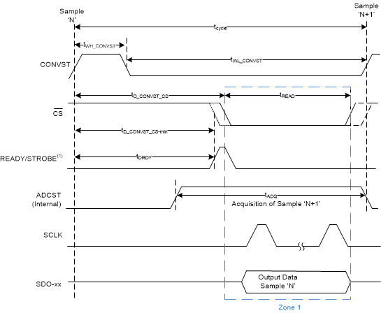
In this mode of conversion control and data transfer, the device starts conversion on the rising edge of CONVST. The CONVST pin can be pulled low after a minimum time of tWH_CONVST. After the conversion is finished, the rising edge of the READY/STROBE pin indicates that the data are ready and the data can be read by the host. After the READY pin is set high, as shown in Figure 44, the host must pull CS low and provide clocks on the SCLK pin to read the data in zone 1 without cycle latency. For a zone 1 transfer, the host must provide a minimum delay time of tD_CONVST_CS (= tDRDY) between the rising edge of CONVST and the falling edge of CS.
The data for the present sample (sample N) is provided by the device on the SDO pins. After all bits are read, the host can pull the CS pin high to end the data transfer frame. After pulling CS high, the host can pull the CONVST pin high to start the next conversion. The host must keep the SDI pin low (NOP0) or high (NOP1) for conversion control and for getting conversion results from the device. In this mode of conversion control, the time between two adjacent rising edges of the CONVST signal (tCYCLE) is determined as tCYCLE = tDRDY + tREAD.
