SBOS588B December 2011 – June 2019 AFE030
PRODUCTION DATA.
- 1 Features
- 2 Applications
- 3 Description
- 4 Revision History
- 5 Description, continued
- 6 Pin Configuration and Functions
-
7 Specifications
- 7.1 Absolute Maximum Ratings
- 7.2 ESD Ratings
- 7.3 Thermal Information
- 7.4 Electrical Characteristics: Transmitter (Tx), Tx_DAC
- 7.5 Electrical Characteristics: Transmitter (Tx), Tx_PGA
- 7.6 Electrical Characteristics: Transmitter (Tx), Tx_FILTER
- 7.7 Electrical Characteristics: Power Amplifier (PA)
- 7.8 Electrical Characteristics: Receiver (Rx), Rx PGA1
- 7.9 Electrical Characteristics: Receiver (Rx), Rx Filter
- 7.10 Electrical Characteristics: Receiver (Rx), Rx PGA2
- 7.11 Electrical Characteristics: Digital
- 7.12 Electrical Characteristics: Two-Wire Interface
- 7.13 Electrical Characteristics: Zero-Crossing Detector
- 7.14 Electrical Characteristics: Internal Bias Generator
- 7.15 Electrical Characteristics: Power Supply
- 7.16 Typical Characteristics
- 8 Parameter Measurement Information
- 9 Detailed Description
- 10Application and Implementation
- 11Device and Documentation Support
Package Options
Mechanical Data (Package|Pins)
- RGZ|48
Thermal pad, mechanical data (Package|Pins)
- RGZ|48
Orderable Information
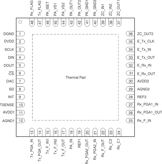
6 Pin Configuration and Functions
RGZ Package
48-Pin VQFN
Top View

Pin Functions
| PIN | I/O | DESCRIPTION | |
|---|---|---|---|
| NAME | NO. | ||
| AGND1 | 12 | — | Analog ground |
| AGND2 | 29 | — | Analog ground |
| AVDD1 | 11 | — | Analog supply |
| AVDD2 | 30 | — | Analog supply |
| CS | 6 | — | SPI digital chip select |
| DAC | 7 | — | DAC mode select |
| DIN | 4 | I | SPI digital input |
| DGND | 1 | — | Digital ground |
| DOUT | 5 | O | SPI digital output |
| DVDD | 2 | — | Digital supply |
| E_Rx_IN | 32 | I | Two-wire receiver input |
| E_Rx_OUT | 31 | O | Two-wire receiver output |
| E_Tx_CLK | 35 | I | Two-wire transmitter clock input |
| E_Tx_IN | 34 | I | Two-wire transmitter input |
| E_Tx_OUT | 33 | O | Two-wire transmitter output |
| INT | 9 | — | Interrupt on overcurrent or thermal limit |
| PA_GND1 | 41 | — | Power amplifier ground |
| PA_GND2 | 40 | — | Power amplifier ground |
| PA_IN | 18 | I | Power amplifier input |
| PA_ISET | 46 | — | Power amplifier current limit set |
| PA_OUT1 | 43 | O | Power amplifier output |
| PA_OUT2 | 42 | O | Power amplifier output |
| PA_VS1 | 45 | — | Power amplifier supply |
| PA_VS2 | 44 | — | Power amplifier supply |
| REF1 | 19 | — | Power amplifier noise reducing capacitor |
| REF2 | 28 | — | Receiver noise reducing capacitor |
| Rx_C1 | 24 | — | Receiver external frequency select |
| Rx_C2 | 23 | — | Receiver external frequency select |
| Rx_F_IN | 25 | I | Receiver filter input |
| Rx_F_OUT | 22 | O | Receiver filter output |
| Rx_FLAG | 48 | — | Receiver ready flag |
| Rx PGA1_IN | 27 | I | Receiver PGA(1) input |
| Rx PGA1_OUT | 26 | O | Receiver PGA(1) output |
| Rx PGA2_IN | 21 | I | Receiver PGA(2) input |
| Rx PGA2_OUT | 20 | O | Receiver PGA(2) output |
| SCLK | 3 | — | SPI serial clock |
| SD | 8 | — | System shutdown |
| TSENSE | 10 | — | Temp sensing diode (anode) |
| Tx_F_IN1 | 15 | I | Transmit filter input 1 |
| Tx_F_IN2 | 16 | I | Transmit filter input 2 |
| Tx_F_OUT | 17 | O | Transmit filter output |
| Tx_FLAG | 47 | — | Transmitter ready flag |
| Tx_PGA_IN | 13 | I | Transmit PGA input |
| Tx_PGA_OUT | 14 | O | Transmit PGA output |
| ZC_IN1 | 39 | I | Zero-crossing detector input |
| ZC_IN2 | 38 | I | Zero-crossing detector input |
| ZC_OUT1 | 37 | O | Zero-crossing detector output |
| ZC_OUT2 | 36 | O | Zero-crossing detector output |