SBOS588B December 2011 – June 2019 AFE030
PRODUCTION DATA.
- 1 Features
- 2 Applications
- 3 Description
- 4 Revision History
- 5 Description, continued
- 6 Pin Configuration and Functions
-
7 Specifications
- 7.1 Absolute Maximum Ratings
- 7.2 ESD Ratings
- 7.3 Thermal Information
- 7.4 Electrical Characteristics: Transmitter (Tx), Tx_DAC
- 7.5 Electrical Characteristics: Transmitter (Tx), Tx_PGA
- 7.6 Electrical Characteristics: Transmitter (Tx), Tx_FILTER
- 7.7 Electrical Characteristics: Power Amplifier (PA)
- 7.8 Electrical Characteristics: Receiver (Rx), Rx PGA1
- 7.9 Electrical Characteristics: Receiver (Rx), Rx Filter
- 7.10 Electrical Characteristics: Receiver (Rx), Rx PGA2
- 7.11 Electrical Characteristics: Digital
- 7.12 Electrical Characteristics: Two-Wire Interface
- 7.13 Electrical Characteristics: Zero-Crossing Detector
- 7.14 Electrical Characteristics: Internal Bias Generator
- 7.15 Electrical Characteristics: Power Supply
- 7.16 Typical Characteristics
- 8 Parameter Measurement Information
- 9 Detailed Description
- 10Application and Implementation
- 11Device and Documentation Support
Package Options
Mechanical Data (Package|Pins)
- RGZ|48
Thermal pad, mechanical data (Package|Pins)
- RGZ|48
Orderable Information
9.5.2 Thermal Overload
The AFE030 contains internal protection circuitry that automatically disables the PA output stage if the junction temperature exceeds +165°C. If a fault condition occurs that causes a thermal overload, and if the T_FLAG_EN bit (location 5 in the Control2 Register) is enabled, the T_FLAG bit (location 5 in the RESET Register) is set to a '1'. This configuration results in an interrupt signal at the INT pin. The AFE030 includes a thermal hysteresis and allows the PA to resume normal operation when the junction temperature reduces to 145°C. The T_FLAG bit remains set to a '1' even after the device returns to normal operation. The T_FLAG bit remains '1' until it is reset by the microprocessor.
If the T_FLAG_EN bit (location 5 in the Control2 Register) is disabled and a thermal overload condition occurs, the PA continues to go into thermal limit and protect the AFE030, but the contents of the T_FLAG bit (location 5 in the RESET Register) remain at the previous value (presumably '0' for normal operation), and the AFE030 does not issue an interrupt at the INT pin.
Once an interrupt is signaled (that is, INT goes low), the contents of the I_FLAG and T_FLAG bits can be read by the microprocessor to determine the type of interrupt that occurred. Using the Control2 Register, each interrupt type (current or thermal) can be individually enabled or disabled, allowing full user customization of the INT function. For proper operation of the interrupt pin it is recommended to configure the interrupt enable registers in the Control2 Register by writing to bit locations 5, 6, and 7 following the information in Table 9 after each time the AFE030 is powered on. Failure to properly configure bit locations 5, 6, and 7 after power on may result in unexpected interrupt signals.
Table 9 lists the register contents associated with each interrupt condition.
Table 9. Register Contents to Configure the Interrupt Pin
| FUNCTION | CONTROL2 REGISTER CONTENTS:
DETERMINE INTERRUPT PIN FUNCTIONALITY |
||
|---|---|---|---|
| I_FLAG_EN
(CURRENT OVERLOAD) |
T_FLAG_EN
(THERMAL OVERLOAD) |
||
| D7 | D6 | D5 | |
| POR (default values) | undefined | 0 | 0 |
| No interrupt | 0 | 0 | 0 |
| Interrupt on thermal overload only | 0 | 0 | 1 |
| Interrupt on current overload only | 0 | 1 | 0 |
| Interrupt on thermal or current overload | 0 | 1 | 1 |
TSENSE Pin (10)
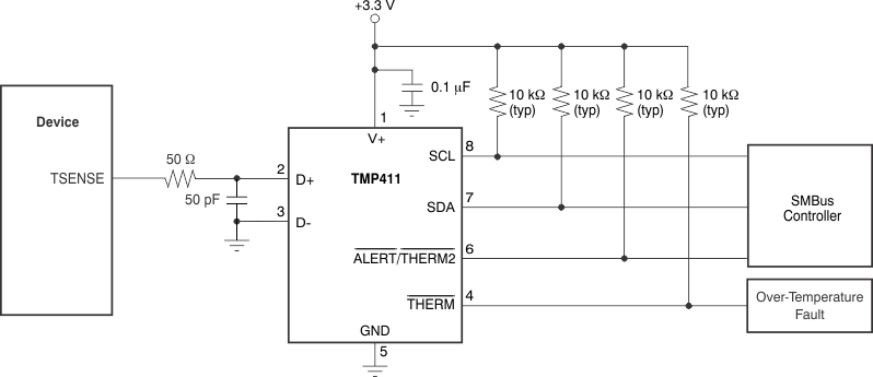
The TSENSE pin is internally connected to the anode of a temperature-sensing diode located within the PA output stage. Figure 45 shows a remote junction temperature sensor circuit that can be used to measure the junction temperature of the AFE030. Measuring the junction temperature of the AFE030 is optional and not required.
 Figure 45. Interfacing the TMP411 to the AFE030
 Tx_FLAG (Pin 47)
The Tx_FLAG pin is an open drain output that indicates the readiness of the Tx signal path for transmission. When the Tx_FLAG pin is high, the transmit signal path is enabled and ready for transmission. When the Tx_FLAG pin is low, the transmit path is not ready for transmission.
Rx_FLAG (Pin 48)
The Rx_FLAG pin is an open drain output that indicates the readiness of the Rx signal path for transmission. When the Rx_FLAG pin is high, the transmit signal path is enabled and ready for transmission. When the Rx_FLAG pin is low, the transmit path is not ready for transmission.