SBOS531E August 2010 – June 2019 AFE031
PRODUCTION DATA.
- 1 Features
- 2 Applications
- 3 Description
- 4 Revision History
- 5 Description, continued
- 6 Device Comparison Table
- 7 Pin Configuration and Functions
-
8 Specifications
- 8.1 Absolute Maximum Ratings
- 8.2 ESD Ratings
- 8.3 Thermal Information
- 8.4 Electrical Characteristics: Transmitter (Tx)
- 8.5 Electrical Characteristics: Power Amplifier (PA)
- 8.6 Electrical Characteristics: Receiver (Rx)
- 8.7 Electrical Characteristics: Digital
- 8.8 Electrical Characteristics: Two-Wire Interface
- 8.9 Electrical Characteristics: Internal Bias Generator
- 8.10 Electrical Characteristics: Power Supply
- 8.11 Timing Requirements
- 8.12 Timing Diagrams
- 8.13 Typical Characteristics
- 9 Detailed Description
- 10Application and Implementation
- 11Device and Documentation Support
- 12Mechanical, Packaging, and Orderable Information
Package Options
Mechanical Data (Package|Pins)
- RGZ|48
Thermal pad, mechanical data (Package|Pins)
Orderable Information
8.13 Typical Characteristics
At TJ = 25°C, PA_VS = 16 V, VAVDD = VDVDD = 3.3 V, and 10 kΩ connected to PA_ISET (pin 46), unless otherwise noted. Figure 5. Tx Filter Gain vs Frequency
  Figure 7. PA Gain vs Frequency
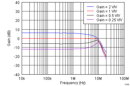
  Figure 9. Tx PGA Gain vs Frequency
  Figure 11. Rx PGA2 Gain vs Frequency
  Figure 13. Filter Cutoff vs Temperature
  Figure 15. PA Gain Error vs Temperature
  Figure 17. Rx PGA2 Gain Error vs Temperature
  Figure 19. Supply Current (Shutdown) vs Temperature
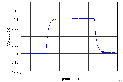
  Figure 21. Tx Filter Pulse Response
  Figure 23. Rx Pulse Response
  Figure 6. Rx Filter Gain vs Frequency
  Figure 8. Maximum PA Output Voltage vs Frequency
  Figure 10. Rx PGA1 Gain vs Frequency
  Figure 12. Two-Wire Receiver Gain vs Frequency
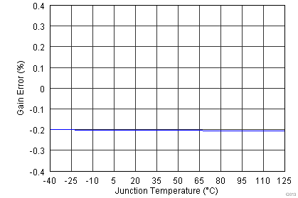
  Figure 14. Tx PGA Gain Error vs Temperature
  Figure 16. Rx PGA1 Gain Error vs Temperature
  Figure 18. Quiescent Supply Current vs Temperature
  Figure 22. PA Pulse Response