SBASB81 December 2024 AFE5401-EP
PRODUCTION DATA
- 1
- 1 Features
- 2 Applications
- 3 Description
- 4 Pin Configuration and Functions
-
5 Specifications
- 5.1 Absolute Maximum Ratings
- 5.2 ESD Ratings
- 5.3 Recommended Operating Conditions
- 5.4 Thermal Information
- 5.5 Electrical Characteristics
- 5.6 Digital Characteristics
- 5.7 Timing Requirements: Output Interface
- 5.8 Timing Requirements: RESET
- 5.9 Timing Requirements: Serial Interface Operation
- 5.10 Typical Characteristics
- 6 Parameter Measurement Information
-
7 Detailed Description
- 7.1 Overview
- 7.2 Functional Block Diagram
- 7.3 Feature Description
- 7.4 Device Functional Modes
- 7.5 Programming
- 7.6 Register Maps
- 8 Application and Implementation
- 9 Revision History
- 10Device and Documentation Support
- 11Mechanical, Packaging, and Orderable Information
Package Options
Mechanical Data (Package|Pins)
- RGC|64
Thermal pad, mechanical data (Package|Pins)
- RGC|64
Orderable Information
7.3.8.1 Main Channels
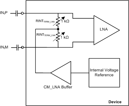
The device analog input consists of a differential LNA. The common-mode for the LNA inputs is internally set using two internal, programmable, single-ended resistors, as shown in Figure 7-7.
 Figure 7-7 Common-Mode Biasing of LNA Input Pins
These resistors can be programmed to a higher value using the TERM_INT_20K_LNA register setting as described in Table 7-8.
| TERM_INT_20K_LNA | DESCRIPTION |
|---|---|
| 0 | RINTTERM_LNA = 1 kΩ |
| 1 | RINTTERM_LNA = 10 kΩ |
Hence, for proper operation, the input signal must be ac-coupled. Note that external input ac-coupling capacitors form a high-pass filter (HPF) with RINTTERM_LNA. Therefore, the capacitor values should allow the lowest frequency of interest to pass with minimum attenuation. For typical frequencies greater than 1 MHz, a value of 50 nF or greater is recommended. The maximum input swing is limited by the LNA gain setting. LNA output swing is limited to 2 VPP before the output becomes saturated or distorted.
Single ended mode of operation is also possible by connecting non-driven input pin to ground through a capacitor of 100 nF. However, this will result in reduced linearity.