SBASB81 December   2024 AFE5401-EP

PRODUCTION DATA  

  1.   1
  2. Features
  3. Applications
  4. Description
  5. Pin Configuration and Functions
    1.     Pin Functions
  6. Specifications
    1. 5.1  Absolute Maximum Ratings
    2. 5.2  ESD Ratings
    3. 5.3  Recommended Operating Conditions
    4. 5.4  Thermal Information
    5. 5.5  Electrical Characteristics
    6. 5.6  Digital Characteristics
    7. 5.7  Timing Requirements: Output Interface
    8. 5.8  Timing Requirements: RESET
    9. 5.9  Timing Requirements: Serial Interface Operation
    10. 5.10 Typical Characteristics
  7. Parameter Measurement Information
    1. 6.1 Timing Requirements: Across Output Serialization Modes
  8. Detailed Description
    1. 7.1 Overview
    2. 7.2 Functional Block Diagram
    3. 7.3 Feature Description
      1. 7.3.1 Low-Noise Amplifier (LNA)
      2. 7.3.2 Programmable Gain Amplifier (PGA)
      3. 7.3.3 Antialiasing Filter
      4. 7.3.4 Analog-to-Digital Converter (ADC)
      5. 7.3.5 Digital Gain
      6. 7.3.6 Input Clock Divider
      7. 7.3.7 Data Output Serialization
      8. 7.3.8 Setting the Input Common-Mode Voltage for the Analog Inputs
        1. 7.3.8.1 Main Channels
        2. 7.3.8.2 Auxiliary Channel
    4. 7.4 Device Functional Modes
      1. 7.4.1 Equalizer Mode
      2. 7.4.2 Data Output Mode
        1. 7.4.2.1 Header
        2. 7.4.2.2 Test Pattern Mode
      3. 7.4.3 Parity
      4. 7.4.4 Standby, Power-Down Mode
      5. 7.4.5 Digital Filtering to Improve Stop-Band Attenuation
        1. 7.4.5.1 Decimate-by-2 Mode
        2. 7.4.5.2 Decimate-by-4 Mode
      6. 7.4.6 Diagnostic Mode
      7. 7.4.7 Signal Chain Probe
    5. 7.5 Programming
      1. 7.5.1 Serial Interface
      2. 7.5.2 Register Initialization
        1. 7.5.2.1 Register Write Mode
        2. 7.5.2.2 Register Read Mode
      3. 7.5.3 CMOS Output Interface
        1. 7.5.3.1 Synchronization and Triggering
    6. 7.6 Register Maps
      1. 7.6.1 Functional Register Map
      2. 7.6.2 Register Descriptions
  9. Application and Implementation
    1. 8.1 Application Information
    2. 8.2 Typical Application
      1. 8.2.1 Design Requirements
      2. 8.2.2 Detailed Design Procedure
      3. 8.2.3 Application Curves
    3. 8.3 Power Supply Recommendations
      1. 8.3.1 Power Supply Sequencing
      2. 8.3.2 Power Supply Decoupling
    4. 8.4 Layout
      1. 8.4.1 Layout Guidelines
      2. 8.4.2 Layout Example
  10. Revision History
  11. 10Device and Documentation Support
    1. 10.1 Documentation Support
      1. 10.1.1 Related Documentation
    2. 10.2 Receiving Notification of Documentation Updates
    3. 10.3 Community Resources
    4. 10.4 Trademarks
  12. 11Mechanical, Packaging, and Orderable Information

Package Options

Mechanical Data (Package|Pins)
Thermal pad, mechanical data (Package|Pins)
Orderable Information

Antialiasing Filter

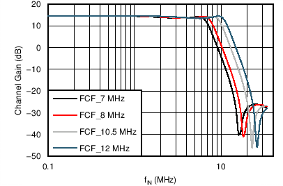
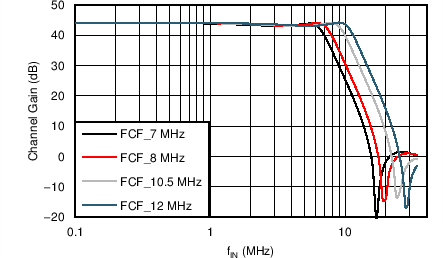
The device introduces a third-order, elliptic, active, antialias, low-pass filter (LPF) in the analog signal path. The filter –3-dB corner frequency can be configured using the FILTER_BW register, as shown in Table 7-3. The corresponding frequency response plots are shown in Figure 7-2 and Figure 7-3.

Table 7-3 FILTER_BW Register
FILTER_BWCORNER FREQUENCY (MHz)
08
17
210.5
312


AFE5401-EP Filter Response Across Modes  (PGA Gain = 0 dB)
Figure 7-2 Filter Response Across Modes (PGA Gain = 0 dB)
AFE5401-EP Filter Response Across Modes  (PGA Gain = 30 dB)
Figure 7-3 Filter Response Across Modes (PGA Gain = 30 dB)