SBASB81 December 2024 AFE5401-EP
PRODUCTION DATA
- 1
- 1 Features
- 2 Applications
- 3 Description
- 4 Pin Configuration and Functions
-
5 Specifications
- 5.1 Absolute Maximum Ratings
- 5.2 ESD Ratings
- 5.3 Recommended Operating Conditions
- 5.4 Thermal Information
- 5.5 Electrical Characteristics
- 5.6 Digital Characteristics
- 5.7 Timing Requirements: Output Interface
- 5.8 Timing Requirements: RESET
- 5.9 Timing Requirements: Serial Interface Operation
- 5.10 Typical Characteristics
- 6 Parameter Measurement Information
-
7 Detailed Description
- 7.1 Overview
- 7.2 Functional Block Diagram
- 7.3 Feature Description
- 7.4 Device Functional Modes
- 7.5 Programming
- 7.6 Register Maps
- 8 Application and Implementation
- 9 Revision History
- 10Device and Documentation Support
- 11Mechanical, Packaging, and Orderable Information
Package Options
Mechanical Data (Package|Pins)
- RGC|64
Thermal pad, mechanical data (Package|Pins)
- RGC|64
Orderable Information
7.3.2 Programmable Gain Amplifier (PGA)
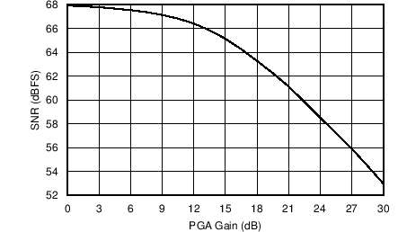
The PGA amplifies the analog input signal by a programmable gain. Gain can be programmed using the PGA_GAIN register, common to all channels, in 3-dB steps with a gain range of 30 dB. In default mode, PGA gain ranges from 0 dB to 30 dB. In equalizer mode, PGA gain ranges from 15 dB to 45 dB. PGA_GAIN register settings are listed in Table 7-2. Figure 7-1 shows the typical SNR values across PGA gain.
Table 7-2 PGA_GAIN Register Settings
| PGA_GAIN Settings | PGA GAIN IN DEFAULT MODE (dB) | PGA GAIN IN EQUALIZER MODE (dB) |
|---|---|---|
| 0 (0 dB) | 0.0 | 15.0 |
| 1 (3 dB) | 2.9 | 17.9 |
| 2 (6 dB) | 6.0 | 21.0 |
| 3 (9 dB) | 8.8 | 23.8 |
| 4 (12 dB) | 11.9 | 26.9 |
| 5 (15 dB) | 14.8 | 29.8 |
| 6 (18 dB) | 17.9 | 32.9 |
| 7 (21 dB) | 20.8 | 35.8 |
| 8 (24 dB) | 23.9 | 38.9 |
| 9 (27 dB) | 26.8 | 41.8 |
| 10 (30 dB) | 29.9 | 44.9 |
 Figure 7-1 SNR Across PGA Gain