SBASB81 December   2024 AFE5401-EP

PRODUCTION DATA  

  1.   1
  2. Features
  3. Applications
  4. Description
  5. Pin Configuration and Functions
    1.     Pin Functions
  6. Specifications
    1. 5.1  Absolute Maximum Ratings
    2. 5.2  ESD Ratings
    3. 5.3  Recommended Operating Conditions
    4. 5.4  Thermal Information
    5. 5.5  Electrical Characteristics
    6. 5.6  Digital Characteristics
    7. 5.7  Timing Requirements: Output Interface
    8. 5.8  Timing Requirements: RESET
    9. 5.9  Timing Requirements: Serial Interface Operation
    10. 5.10 Typical Characteristics
  7. Parameter Measurement Information
    1. 6.1 Timing Requirements: Across Output Serialization Modes
  8. Detailed Description
    1. 7.1 Overview
    2. 7.2 Functional Block Diagram
    3. 7.3 Feature Description
      1. 7.3.1 Low-Noise Amplifier (LNA)
      2. 7.3.2 Programmable Gain Amplifier (PGA)
      3. 7.3.3 Antialiasing Filter
      4. 7.3.4 Analog-to-Digital Converter (ADC)
      5. 7.3.5 Digital Gain
      6. 7.3.6 Input Clock Divider
      7. 7.3.7 Data Output Serialization
      8. 7.3.8 Setting the Input Common-Mode Voltage for the Analog Inputs
        1. 7.3.8.1 Main Channels
        2. 7.3.8.2 Auxiliary Channel
    4. 7.4 Device Functional Modes
      1. 7.4.1 Equalizer Mode
      2. 7.4.2 Data Output Mode
        1. 7.4.2.1 Header
        2. 7.4.2.2 Test Pattern Mode
      3. 7.4.3 Parity
      4. 7.4.4 Standby, Power-Down Mode
      5. 7.4.5 Digital Filtering to Improve Stop-Band Attenuation
        1. 7.4.5.1 Decimate-by-2 Mode
        2. 7.4.5.2 Decimate-by-4 Mode
      6. 7.4.6 Diagnostic Mode
      7. 7.4.7 Signal Chain Probe
    5. 7.5 Programming
      1. 7.5.1 Serial Interface
      2. 7.5.2 Register Initialization
        1. 7.5.2.1 Register Write Mode
        2. 7.5.2.2 Register Read Mode
      3. 7.5.3 CMOS Output Interface
        1. 7.5.3.1 Synchronization and Triggering
    6. 7.6 Register Maps
      1. 7.6.1 Functional Register Map
      2. 7.6.2 Register Descriptions
  9. Application and Implementation
    1. 8.1 Application Information
    2. 8.2 Typical Application
      1. 8.2.1 Design Requirements
      2. 8.2.2 Detailed Design Procedure
      3. 8.2.3 Application Curves
    3. 8.3 Power Supply Recommendations
      1. 8.3.1 Power Supply Sequencing
      2. 8.3.2 Power Supply Decoupling
    4. 8.4 Layout
      1. 8.4.1 Layout Guidelines
      2. 8.4.2 Layout Example
  10. Revision History
  11. 10Device and Documentation Support
    1. 10.1 Documentation Support
      1. 10.1.1 Related Documentation
    2. 10.2 Receiving Notification of Documentation Updates
    3. 10.3 Community Resources
    4. 10.4 Trademarks
  12. 11Mechanical, Packaging, and Orderable Information

Package Options

Mechanical Data (Package|Pins)
Thermal pad, mechanical data (Package|Pins)
Orderable Information

Typical Application

As Figure 8-1 illustrates, the device also consists of four auxiliary channels, where the analog signal chain (LNA, PGA) is bypassed and the analog inputs can be directly digitized. This configuration is very useful in the system to digitize monitoring signals (such as battery voltages and temperature sensor outputs).

As the Section 8.2.1 section describes, the device can accept a variety of input clock signals (such as differential sine-wave, LVPECL, or LVDS). The can also functions seamlessly with a single-ended LVCMOS (1.8 V) clock input.

The device is designed to have a simple CMOS output data interface. Used with the TRIG and DSYNCx signals, the device can be interfaced to standard video ports of DSPs and other field-programmable gate array (FPGA) and micro-controller based receivers.
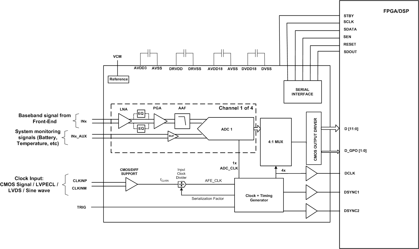
AFE5401-EP Typical Application DiagramFigure 8-1 Typical Application Diagram