SBASB81 December 2024 AFE5401-EP
PRODUCTION DATA
- 1
- 1 Features
- 2 Applications
- 3 Description
- 4 Pin Configuration and Functions
-
5 Specifications
- 5.1 Absolute Maximum Ratings
- 5.2 ESD Ratings
- 5.3 Recommended Operating Conditions
- 5.4 Thermal Information
- 5.5 Electrical Characteristics
- 5.6 Digital Characteristics
- 5.7 Timing Requirements: Output Interface
- 5.8 Timing Requirements: RESET
- 5.9 Timing Requirements: Serial Interface Operation
- 5.10 Typical Characteristics
- 6 Parameter Measurement Information
-
7 Detailed Description
- 7.1 Overview
- 7.2 Functional Block Diagram
- 7.3 Feature Description
- 7.4 Device Functional Modes
- 7.5 Programming
- 7.6 Register Maps
- 8 Application and Implementation
- 9 Revision History
- 10Device and Documentation Support
- 11Mechanical, Packaging, and Orderable Information
Package Options
Mechanical Data (Package|Pins)
- RGC|64
Thermal pad, mechanical data (Package|Pins)
- RGC|64
Orderable Information
7.4.2.1 Header
Each channel has an associated 12-bit header register. These registers can be written by an SPI write. The content of this register can be read out on the CMOS data output (D[11:0]) by configuring the HEADER_MODE register, as shown in Table 7-18.
Table 7-18 HEADER_MODE Register
| HEADER_MODE | DESCRIPTION |
|---|---|
| 0 | ADC data at output |
| 1 | Header data at output |
| 2 | [Temperature data, diagnostic data, mean, noise, (-1), (-1), (-1), (-1)]. This data sequence is repeated. |
| 3 | Header data, temperature data, diagnostic data, mean, noise, ADC data |
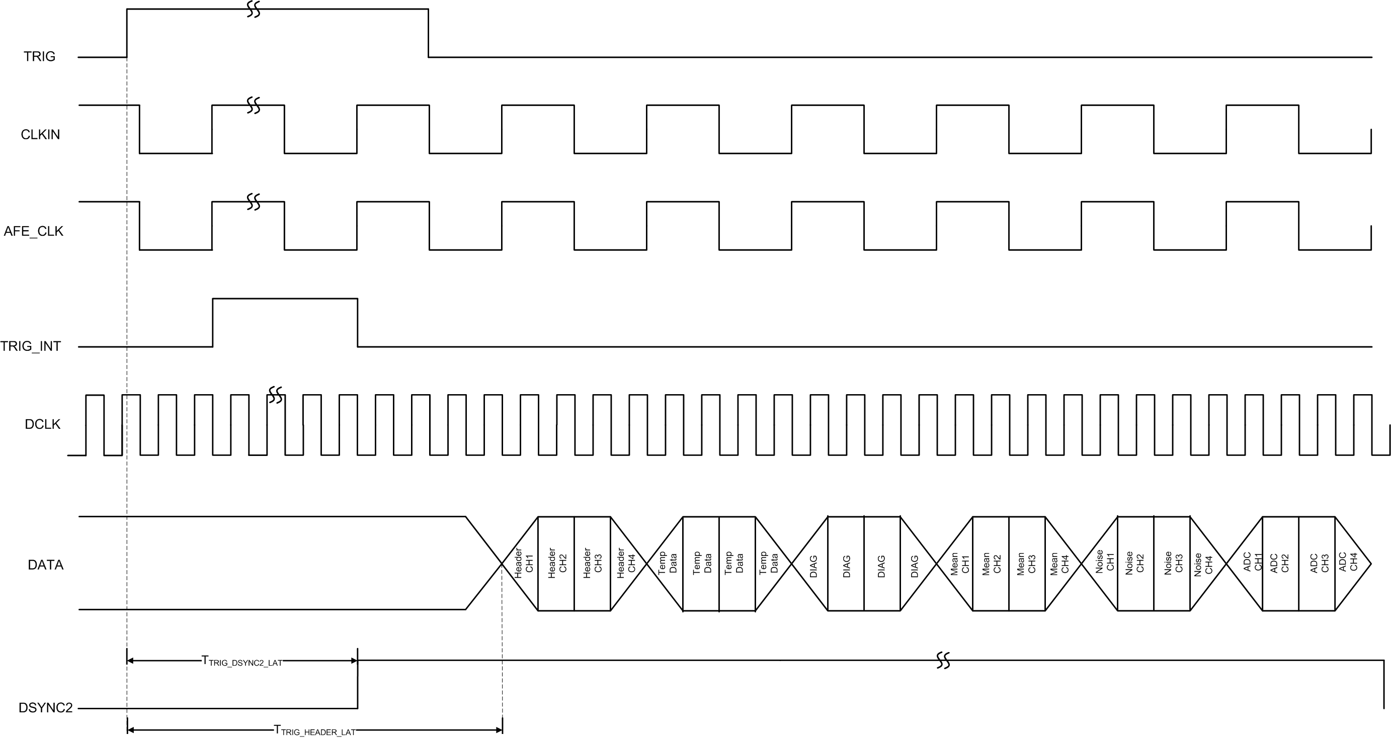
In HEADER_MODE = 3, the header mode data output is shown in Figure 7-14.
In this mode, header data is transmitted with a latency with respect to the TRIG input. This latency is given by Equation 2:
Equation 2. TRIG to Header Latency (TTRIG_HEADER_LAT) = tAFE_CLK + TTRIG_DSYNC2_LAT
 Figure 7-14 Header Mode Data Output (HEADER_MODE = 3)