SBASB81 December 2024 AFE5401-EP
PRODUCTION DATA
- 1
- 1 Features
- 2 Applications
- 3 Description
- 4 Pin Configuration and Functions
-
5 Specifications
- 5.1 Absolute Maximum Ratings
- 5.2 ESD Ratings
- 5.3 Recommended Operating Conditions
- 5.4 Thermal Information
- 5.5 Electrical Characteristics
- 5.6 Digital Characteristics
- 5.7 Timing Requirements: Output Interface
- 5.8 Timing Requirements: RESET
- 5.9 Timing Requirements: Serial Interface Operation
- 5.10 Typical Characteristics
- 6 Parameter Measurement Information
-
7 Detailed Description
- 7.1 Overview
- 7.2 Functional Block Diagram
- 7.3 Feature Description
- 7.4 Device Functional Modes
- 7.5 Programming
- 7.6 Register Maps
- 8 Application and Implementation
- 9 Revision History
- 10Device and Documentation Support
- 11Mechanical, Packaging, and Orderable Information
Package Options
Mechanical Data (Package|Pins)
- RGC|64
Thermal pad, mechanical data (Package|Pins)
- RGC|64
Orderable Information
7.5.3.1 Synchronization and Triggering
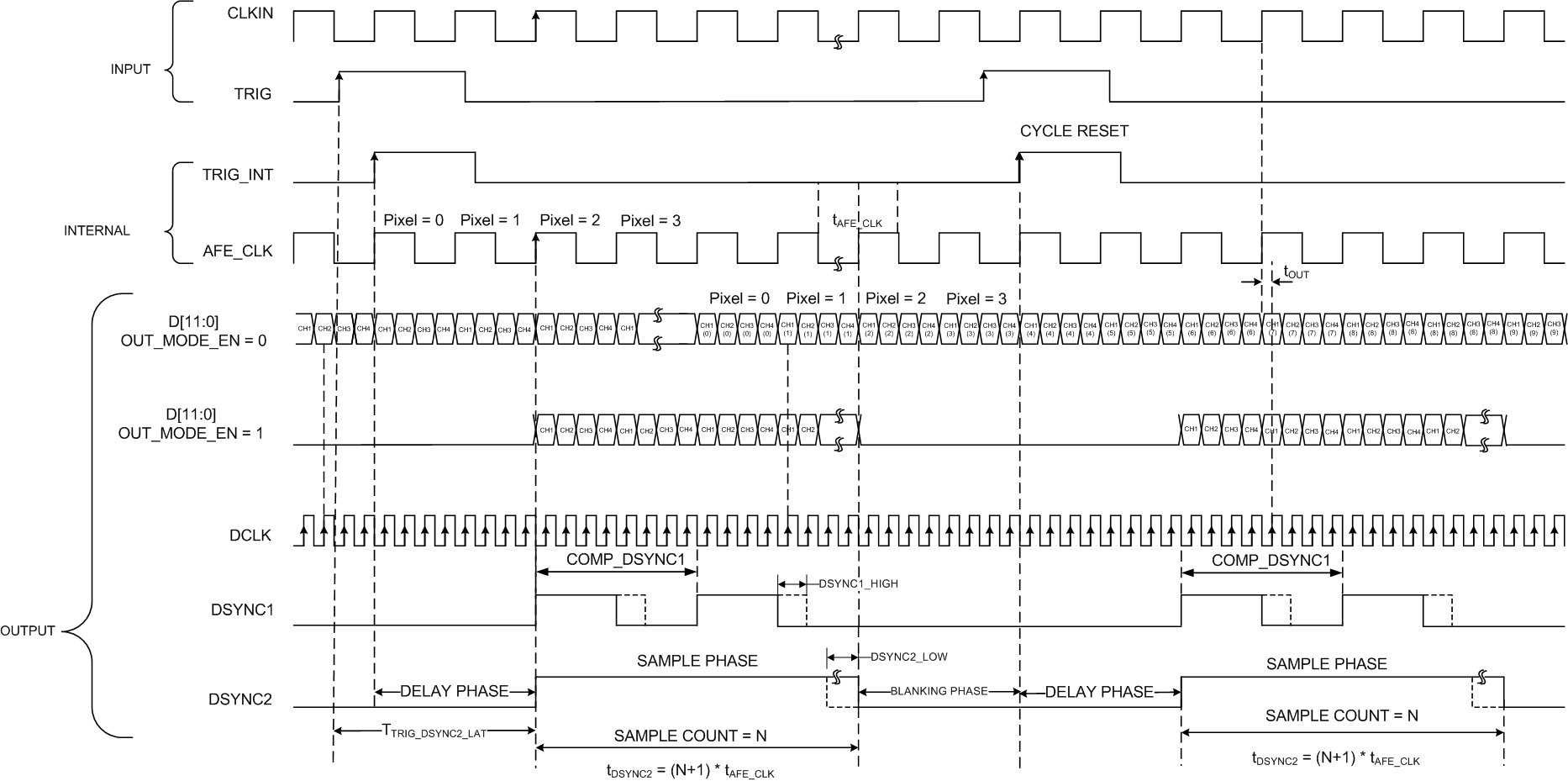
While the digital data from the four channels is multiplexed on the output bus, some mechanism is required to identify the data from the individual channels. Other than the output data and DCLK, the device also outputs DSYNCx signals that can be used for channel identification.
The DSYNCx output signals function with the TRIG input signal. Every time that a trigger pulse is received on the TRIG pin, the device outputs the DSYNC1 and DSYNC2 signals. The DSYNCx signals can be configured in the following ways:
- The delay between the arrival of the TRIG signal and the DSYNCx signal becoming active is programmable in a number of AFE_CLK cycles (using the DELAY_COUNT register bit).
- The period of the DSYNC1 signal is programmable in terms of AFE_CLK clock cycles by using the COMP_DSYNC1 register bits.
- The active time of the DSYNC2 signal is programmable using the SAMPLE_COUNT register bits.
The rising edge of the DSYNC1 signal coincides with the channel 1 data, as shown in Figure 7-22. This occurrence can be used by the receiving device to identify individual channels.
The sample phase period corresponds to the period when valid data is available from the device when OUT_MODE_EN = 1.
 Figure 7-22 DSYNCx Timing Diagram