SBASB81 December 2024 AFE5401-EP
PRODUCTION DATA
- 1
- 1 Features
- 2 Applications
- 3 Description
- 4 Pin Configuration and Functions
-
5 Specifications
- 5.1 Absolute Maximum Ratings
- 5.2 ESD Ratings
- 5.3 Recommended Operating Conditions
- 5.4 Thermal Information
- 5.5 Electrical Characteristics
- 5.6 Digital Characteristics
- 5.7 Timing Requirements: Output Interface
- 5.8 Timing Requirements: RESET
- 5.9 Timing Requirements: Serial Interface Operation
- 5.10 Typical Characteristics
- 6 Parameter Measurement Information
-
7 Detailed Description
- 7.1 Overview
- 7.2 Functional Block Diagram
- 7.3 Feature Description
- 7.4 Device Functional Modes
- 7.5 Programming
- 7.6 Register Maps
- 8 Application and Implementation
- 9 Revision History
- 10Device and Documentation Support
- 11Mechanical, Packaging, and Orderable Information
Package Options
Mechanical Data (Package|Pins)
- RGC|64
Thermal pad, mechanical data (Package|Pins)
- RGC|64
Orderable Information
5.9 Timing Requirements: Serial Interface Operation
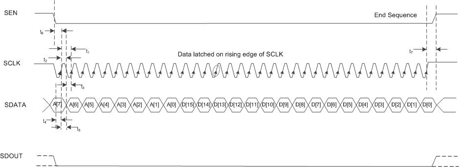
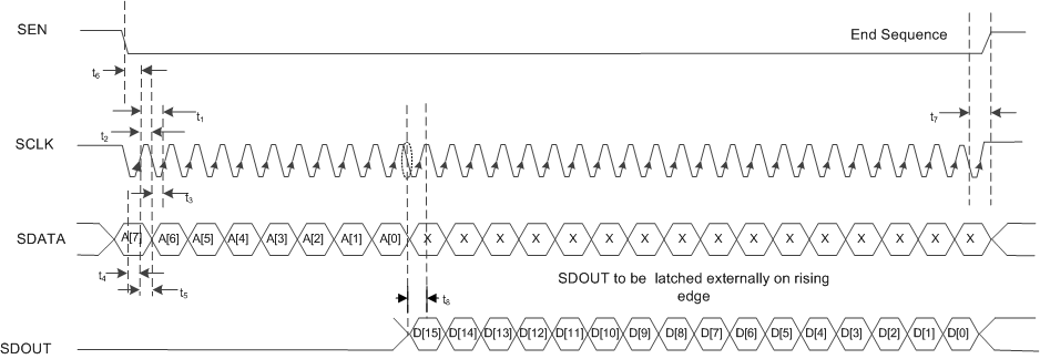
Minimum specifications are across the full temperature range of TA = –40°C to TJ = +125°C, DRVDD = 3.3 V, AVDD3 = 3.3 V, AVDD18 = 1.8 V, and DVDD18 = 1.8 V, CLOAD on SDOUT = 5 pF, unless otherwise noted.
| PARAMETER | MIN | TYP | MAX | UNIT | |
|---|---|---|---|---|---|
| t1 | SCLK period | 50 | ns | ||
| t2 | SCLK high time | 20 | ns | ||
| t3 | SCLK low time | 20 | ns | ||
| t4 | Data setup time | 5 | ns | ||
| t5 | Data hold time | 5 | ns | ||
| t6 | SEN falling to SCLK rising | 8 | ns | ||
| t7 | Time between last SCLK rising edge to SEN rising edge | 8 | ns | ||
| t8 | Delay from SCLK falling edge to SDOUT valid | 7 | 11 | 15 | ns |

A. tCLK = 1 / fCLKIN
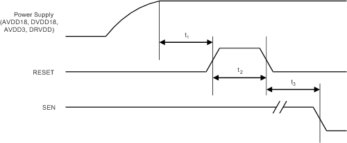
Figure 5-1 Output Interface Timing DiagramA high pulse on the RESET pin is required for register initialization through the reset pin. Figure 5-2 shows the timing requirement for reset after power-up.
 Figure 5-2 Reset Timing
 Figure 5-3 Serial Interface Register Write Timing Diagram
 Figure 5-4 Serial Interface Register Readout Timing Diagram