SBASB81 December 2024 AFE5401-EP
PRODUCTION DATA
- 1
- 1 Features
- 2 Applications
- 3 Description
- 4 Pin Configuration and Functions
-
5 Specifications
- 5.1 Absolute Maximum Ratings
- 5.2 ESD Ratings
- 5.3 Recommended Operating Conditions
- 5.4 Thermal Information
- 5.5 Electrical Characteristics
- 5.6 Digital Characteristics
- 5.7 Timing Requirements: Output Interface
- 5.8 Timing Requirements: RESET
- 5.9 Timing Requirements: Serial Interface Operation
- 5.10 Typical Characteristics
- 6 Parameter Measurement Information
-
7 Detailed Description
- 7.1 Overview
- 7.2 Functional Block Diagram
- 7.3 Feature Description
- 7.4 Device Functional Modes
- 7.5 Programming
- 7.6 Register Maps
- 8 Application and Implementation
- 9 Revision History
- 10Device and Documentation Support
- 11Mechanical, Packaging, and Orderable Information
Package Options
Mechanical Data (Package|Pins)
- RGC|64
Thermal pad, mechanical data (Package|Pins)
- RGC|64
Orderable Information
7.4.2 Data Output Mode
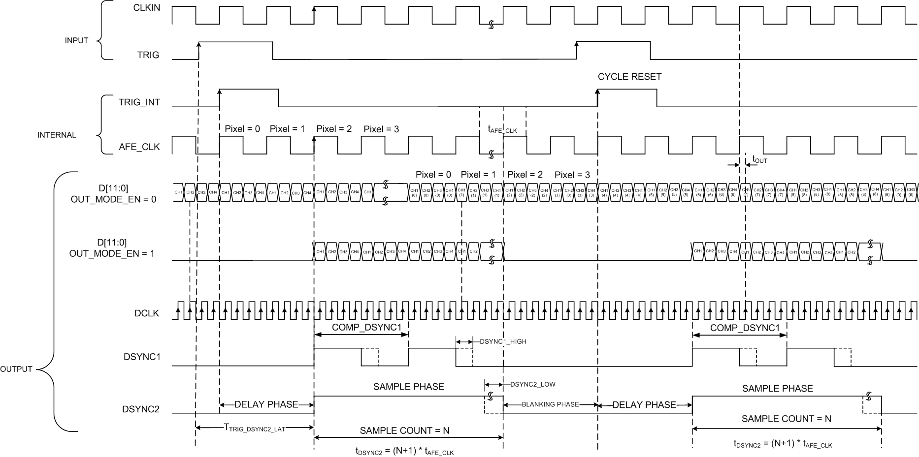
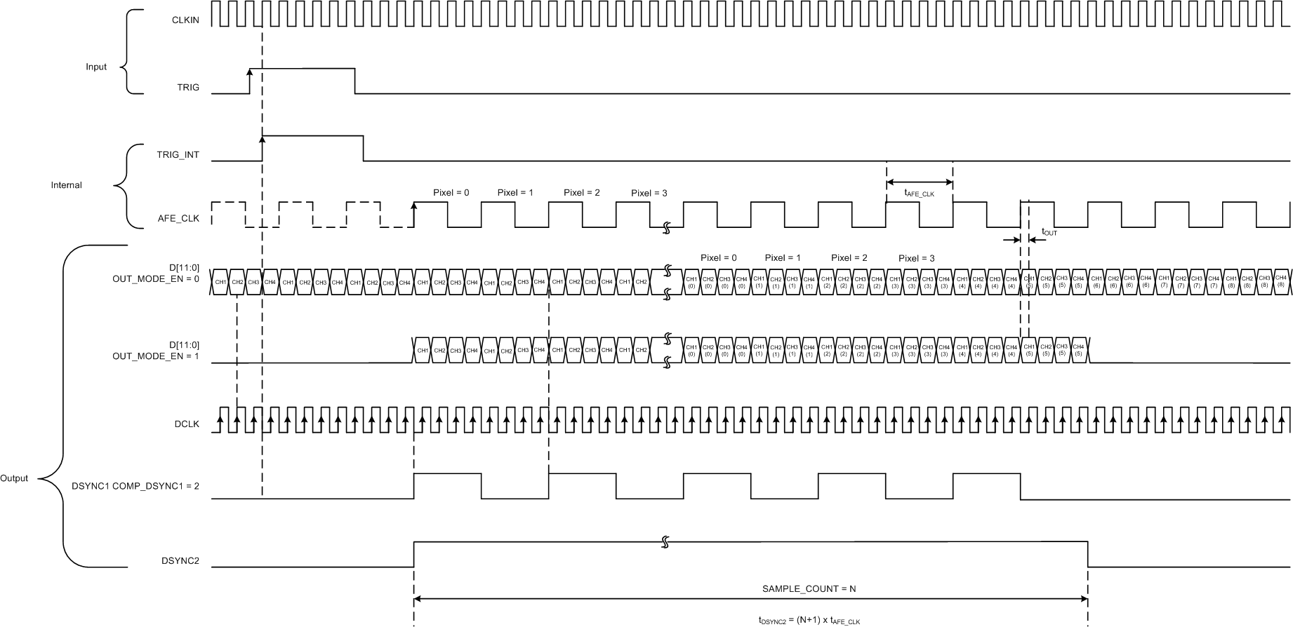
The functionality of DSYNC1, DSYNC2, DCLK, and D[11:0] are controlled by selecting the data output mode. The functionality of the DSYNC1, DSYNC2, DCLK, and D[11:0] output pins for 4x serialization modes are shown in Figure 7-11 and Figure 7-12. Any event on the TRIG pin triggers the DSYNC1 and DSYNC2 signals. The DSYNC1 period is determined by the COMP_DSYNC1 register value and the DSYNC2 period is determined by the SAMPLE_COUNT register value. When OUT_MODE_EN = 0, data output is continuous. When OUT_MODE_EN = 1, data is active only during the sample phase. Output pins are configured using the registers described in Table 7-12 through Table 7-16.
 Figure 7-11 Data Output Timing Diagram (4x Serialization)
 Figure 7-12 Data Output Timing Diagram (4x Serialization, Input Divider Enabled)
| REGISTER | FUNCTION |
|---|---|
| DELAY_COUNT[23:0] | From a TRIG event, the sample phase is delayed for a DELAY_COUNT number of tAFE_CLK cycles |
| SAMPLE_COUNT[23:0] | From the end of DELAY_PHASE, the sample phase duration is the SAMPLE_COUNT number of tAFE_CLK cycles |
| COMP_DSYNC1[15:0] | DSYNC1 period in number of tAFE_CLKcycles |
| DSYNC1_START_LOW | DESCRIPTION |
|---|---|
| 0 | DSYNC1 is high at the sample phase start |
| 1 | DSYNC1 is low at the sample phase start |
| OUT_MODE_EN | DESCRIPTION |
|---|---|
| 0 | Data always active |
| 1 | Data active in sample phase |
| DSYNC_EN | DESCRIPTION |
|---|---|
| 0 | Disable DSYNC generation |
| 1 | Enable DSYNC generation |
| OUT_BLANK_HIZ | DESCRIPTION |
|---|---|
| 0 | D[11:0] is low during inactive phase |
| 1 | D[11:0] is high impedance during inactive phase |
The signal processing blocks in the device are always active and are not controlled by output mode configuration settings.
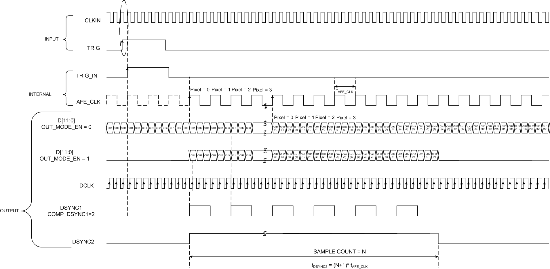
The functionality of the DSYNC1, DSYNC2, DCLK, and D[11:0] output pins with the input divider enabled for 3x serializations is shown in Figure 7-13.
 Figure 7-13 Data Output Timing (3x Serialization, Input Divider Enabled)
The TRIG to DSYNC2 latency is given by Table 7-17.
| Serialization Modes | TTRIG_DSYNC2_LAT(1) | Units |
|---|---|---|
| 4x | 230 | ns |
| 3x | 230 | ns |
| 2x | 240 | ns |
| 1x | 250 | ns |