SBASB81 December 2024 AFE5401-EP
PRODUCTION DATA
- 1
- 1 Features
- 2 Applications
- 3 Description
- 4 Pin Configuration and Functions
-
5 Specifications
- 5.1 Absolute Maximum Ratings
- 5.2 ESD Ratings
- 5.3 Recommended Operating Conditions
- 5.4 Thermal Information
- 5.5 Electrical Characteristics
- 5.6 Digital Characteristics
- 5.7 Timing Requirements: Output Interface
- 5.8 Timing Requirements: RESET
- 5.9 Timing Requirements: Serial Interface Operation
- 5.10 Typical Characteristics
- 6 Parameter Measurement Information
-
7 Detailed Description
- 7.1 Overview
- 7.2 Functional Block Diagram
- 7.3 Feature Description
- 7.4 Device Functional Modes
- 7.5 Programming
- 7.6 Register Maps
- 8 Application and Implementation
- 9 Revision History
- 10Device and Documentation Support
- 11Mechanical, Packaging, and Orderable Information
Package Options
Mechanical Data (Package|Pins)
- RGC|64
Thermal pad, mechanical data (Package|Pins)
- RGC|64
Orderable Information
8.2.2 Detailed Design Procedure
For the LVDS input clock, RTERM = 100 Ω is recommended. For the LVPECL clock input, RTERM must be determined based on the LVPECL driver recommendations. To operate using a single-ended clock, connect a CMOS clock source to CLKINP and tie CLKINM to GND. The device automatically detects the presence of a single-ended clock without requiring any configuration and disables internal biasing. Typical clock termination schemes are illustrated in Figure 8-4, Figure 8-5, Figure 8-6, and Figure 8-7. Typical characteristic plots across input clock amplitude and duty cycle are shown in Section 8.2.3.
Figure 8-2 and Figure 8-3 illustrate the equivalent circuits of the clock input pins for Differential and Single-Ended input clock respectively.
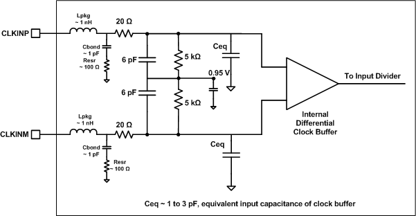 Figure 8-2 Clock Input Equivalent Circuit (Differential Mode)
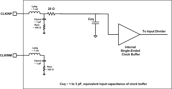 Figure 8-3 Clock Input Equivalent Circuit (Single-Ended Mode)
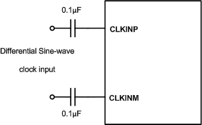 Figure 8-4 Differential Sine-Wave Clock Driving Circuit
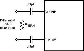 Figure 8-6 Differential LVDS Clock Driving Circuit
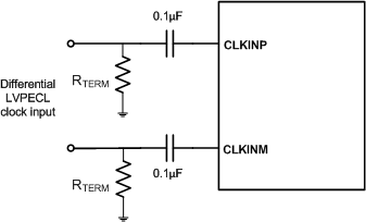 Figure 8-5 Differential LVPECL Clock Driving Circuit
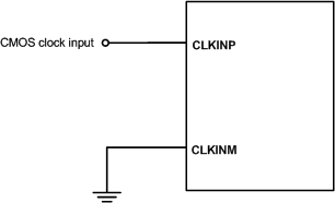 Figure 8-7 Single-Ended Clock Driving Circuit