SLASF21 December   2022 AFE78101 , AFE88101

PRODUCTION DATA  

  1. Features
  2. Applications
  3. Description
  4. Revision History
  5. Pin Configuration and Functions
  6. Specifications
    1. 6.1  Absolute Maximum Ratings
    2. 6.2  ESD Ratings
    3. 6.3  Recommended Operating Conditions
    4. 6.4  Thermal Information
    5. 6.5  Electrical Characteristics
    6. 6.6  Timing Requirements
    7. 6.7  Timing Diagrams
    8. 6.8  Typical Characteristics: VOUT DAC
    9. 6.9  Typical Characteristics: ADC
    10. 6.10 Typical Characteristics: Reference
    11. 6.11 Typical Characteristics: Power Supply
  7. Detailed Description
    1. 7.1 Overview
    2. 7.2 Functional Block Diagram
    3. 7.3 Feature Description
      1. 7.3.1 Digital-to-Analog Converter (DAC) Overview
        1. 7.3.1.1 DAC Resistor String
        2. 7.3.1.2 DAC Buffer Amplifier
        3. 7.3.1.3 DAC Transfer Function
        4. 7.3.1.4 DAC Gain and Offset Calibration
        5. 7.3.1.5 Programmable Slew Rate
        6. 7.3.1.6 DAC Register Structure and CLEAR State
      2. 7.3.2 Analog-to-Digital Converter (ADC) Overview
        1. 7.3.2.1 ADC Operation
        2. 7.3.2.2 ADC Custom Channel Sequencer
        3. 7.3.2.3 ADC Synchronization
        4. 7.3.2.4 ADC Offset Calibration
        5. 7.3.2.5 External Monitoring Inputs
        6. 7.3.2.6 Temperature Sensor
        7. 7.3.2.7 Self-Diagnostic Multiplexer
        8. 7.3.2.8 ADC Bypass
      3. 7.3.3 Programmable Out-of-Range Alarms
        1. 7.3.3.1 Alarm Action Configuration Register
        2. 7.3.3.2 Alarm Voltage Generator
        3. 7.3.3.3 Temperature Sensor Alarm Function
        4. 7.3.3.4 Internal Reference Alarm Function
        5. 7.3.3.5 ADC Alarm Function
        6. 7.3.3.6 Fault Detection
      4. 7.3.4 IRQ
      5. 7.3.5 Internal Reference
      6. 7.3.6 Integrated Precision Oscillator
      7. 7.3.7 One-Time Programmable (OTP) Memory
    4. 7.4 Device Functional Modes
      1. 7.4.1 DAC Power-Down Mode
      2. 7.4.2 Reset
    5. 7.5 Programming
      1. 7.5.1 Communication Setup
        1. 7.5.1.1 SPI Mode
        2. 7.5.1.2 UART Mode
      2. 7.5.2 Serial Peripheral Interface (SPI)
        1. 7.5.2.1 SPI Frame Definition
        2. 7.5.2.2 SPI Read and Write
        3. 7.5.2.3 Frame Error Checking
        4. 7.5.2.4 Synchronization
      3. 7.5.3 UART
        1. 7.5.3.1 UART Break Mode (UBM)
      4. 7.5.4 Status Bits
      5. 7.5.5 Watchdog Timer
    6. 7.6 Register Maps
      1. 7.6.1 AFEx8101 Registers
  8. Application and Implementation
    1. 8.1 Application Information
      1. 8.1.1 Multichannel Configuration
    2. 8.2 Typical Application
      1. 8.2.1 4-mA to 20-mA Current Transmitter
        1. 8.2.1.1 Design Requirements
        2. 8.2.1.2 Detailed Design Procedure
          1. 8.2.1.2.1 Start-Up Circuit
          2. 8.2.1.2.2 Current Loop Control
          3. 8.2.1.2.3 Input Protection and Rectification
          4. 8.2.1.2.4 System Current Budget
        3. 8.2.1.3 Application Curves
    3. 8.3 Initialization Set Up
    4. 8.4 Power Supply Recommendations
    5. 8.5 Layout
      1. 8.5.1 Layout Guidelines
      2. 8.5.2 Layout Example
  9. Device and Documentation Support
    1. 9.1 Documentation Support
      1. 9.1.1 Related Documentation
    2. 9.2 Receiving Notification of Documentation Updates
    3. 9.3 Support Resources
    4. 9.4 Trademarks
    5. 9.5 Electrostatic Discharge Caution
    6. 9.6 Glossary
  10. 10Mechanical, Packaging, and Orderable Information

Package Options

Mechanical Data (Package|Pins)
Thermal pad, mechanical data (Package|Pins)
Orderable Information

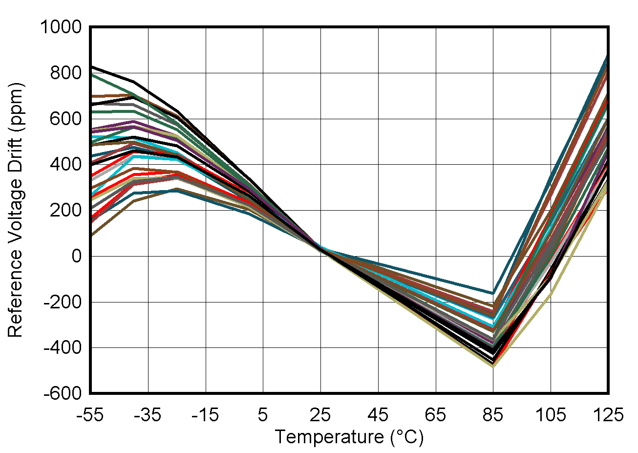
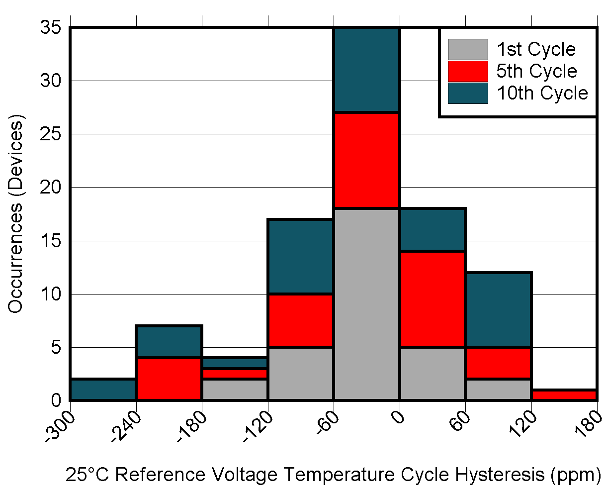
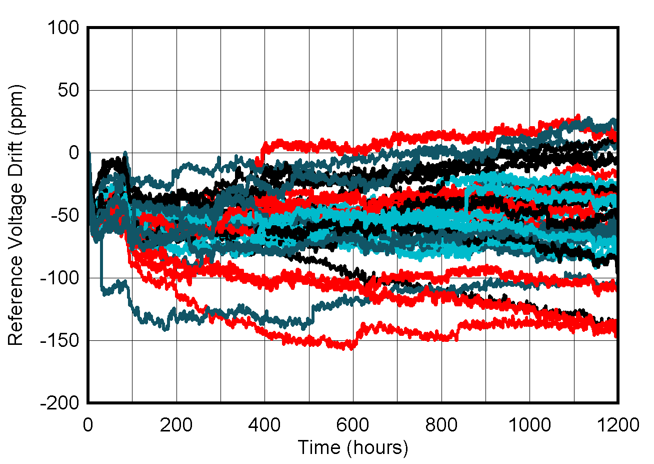
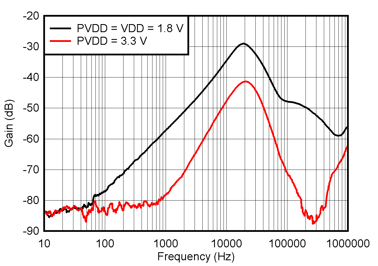
Typical Characteristics: Reference

at TA = 25°C, PVDD = IOVDD = 3.3 V, external or internal VREFIO = 1.25 V, RLOAD = 50 kΩ to GND, CLOAD = 100 pF to GND, and digital inputs at IOVDD or GND (unless otherwise noted)
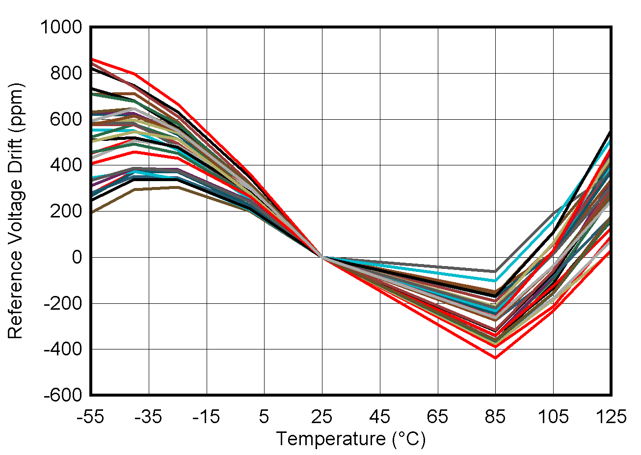
GUID-20220927-SS0I-WGSP-XV2T-RN71JQLQ4BVR-low.png
Pre-soldered
Figure 6-41 Reference Voltage Temperature Drift
GUID-20221026-SS0I-FTM1-4FSK-SFJC564NGXNX-low.png
 
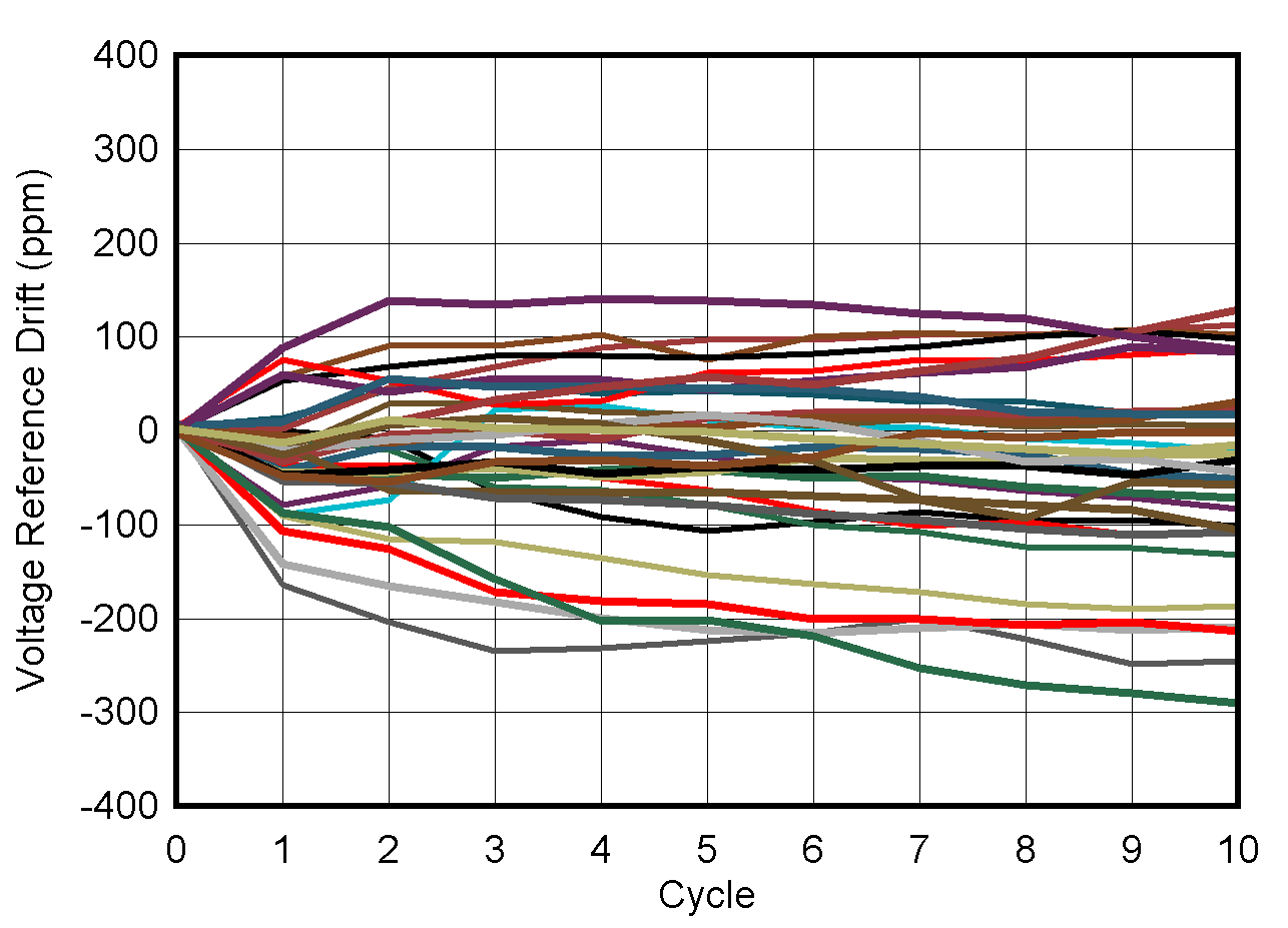
–40°C to +85°C cycles, 60 minutes per cycle
Figure 6-43 Multiple Temperature Cycle Hysteresis
GUID-20220927-SS0I-HBD6-58PG-70RXVBSNDVMH-low.png
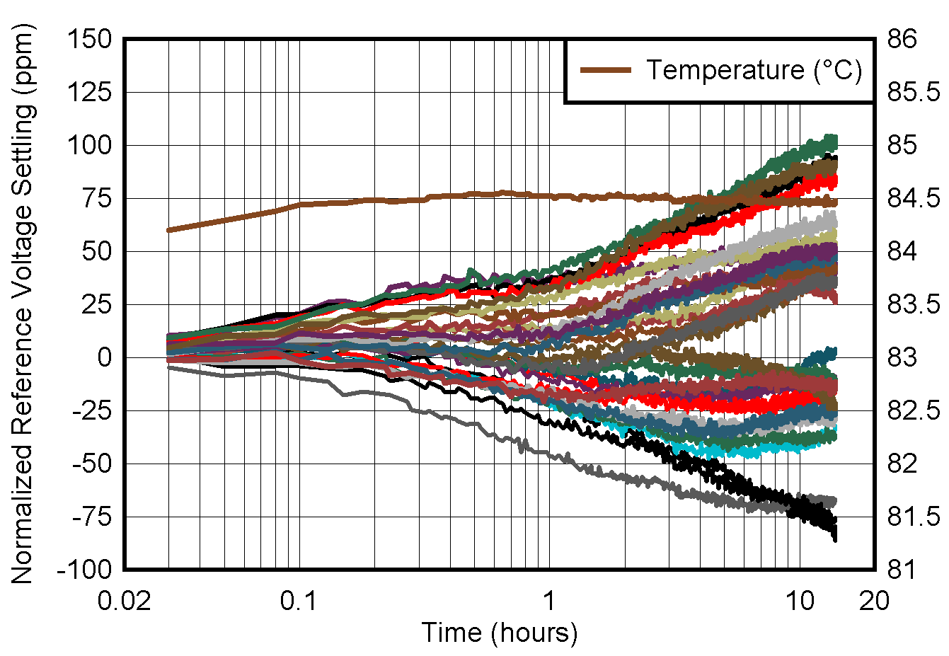
Two minutes after 25°C to 85°C temperature step
Figure 6-45 Ambient Temperature Change Settling
GUID-20220618-SS0I-HVTD-8LRL-PHZLDWS3CGH1-low.png
 
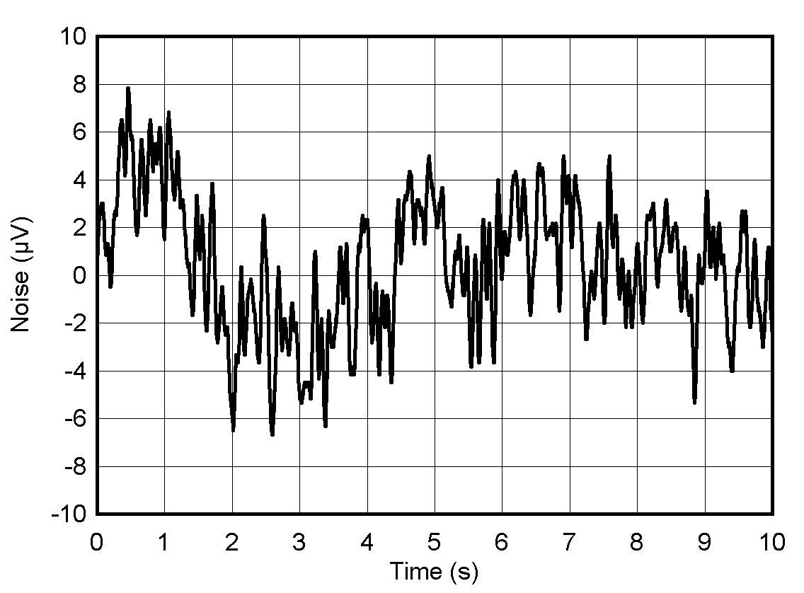
Figure 6-47 Reference Output Noise, 0.1 Hz to 10 Hz
GUID-20220618-SS0I-TLQK-3KKQ-3W2T63G2DP0Z-low.png
 
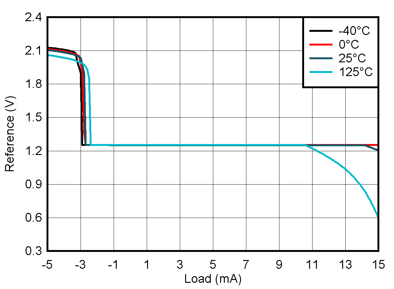
Figure 6-49 Reference Source and Sink Current Capability
GUID-20220927-SS0I-W4HB-DC7D-6WWRH8L9S85Z-low.png
Post-soldered
Figure 6-42 Reference Voltage Temperature Drift
GUID-20220927-SS0I-GR9J-DQ4V-8RBDPZZLN3DF-low.png
–40°C to +85°C cycles, 60 minutes per cycle
Figure 6-44 Multiple Temperature Cycle Hysteresis
GUID-20220927-SS0I-1K1S-K8KL-PVCSBGVGJ9BM-low.png
 
Figure 6-46 Reference Voltage Long-Term Stability
GUID-20220618-SS0I-K6B5-ZJB4-1MZSCV664KH8-low.png
 
Figure 6-48 Reference AC PSRR vs frequency
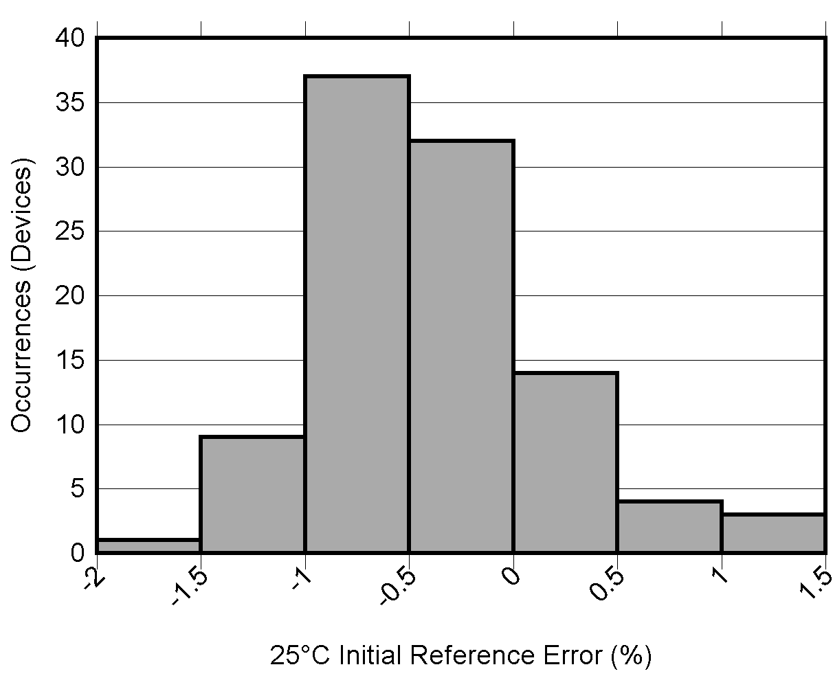
GUID-20221026-SS0I-P2HC-BDSG-CRZFHKCRHVTC-low.pngFigure 6-50 Initial Accuracy Distribution