Typical values at TA = +25°C with
nominal supplies. Default conditions: TX input data rate = 491.52MSPS,
fDAC = 11796.48 MSPS (24x interpolation), interleave mode,
1st Nyquist zone output, PLL clock mode with fREF = 491.52
MHz, AOUT = –1 dBFS, DSA = 0 dB, Sin(x)/x enabled, DSA calibrated

| Aout = -0.5dFBS, 3.5 GHz Matching,
included PCB and cable losses |
|
|
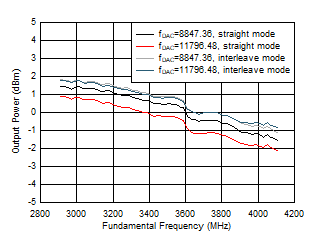
Figure 5-118 TX
Output Power vs Frequency
| 3.5
GHz Matching, included PCB and cable losses |
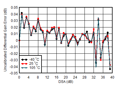
| Differential Gain Error = POUT(DSA Setting –
1) – POUT(DSA Setting) + 1 |
Figure 5-120 TX
Uncalibrated Differential Gain Error vs DSA Setting and Channel at 3.5
GHz
| 3.5
GHz Matching, included PCB and cable losses |
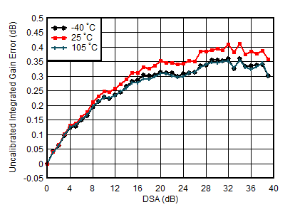
| Integrated Gain Error = POUT(DSA Setting) –
POUT(DSA Setting = 0) + (DSA
Setting) |
Figure 5-122 TX
Uncalibrated Integrated Gain Error vs DSA Setting and Channel at 3.5
GHz
| 3.5
GHz Matching, included PCB and cable losses |
|
|
Figure 5-124 TX
Uncalibrated Differential Phase Error vs DSA Setting and Channel at 3.5
GHz
| 3.5
GHz Matching, included PCB and cable losses |
Figure 5-126 TX
Uncalibrated Integrated Phase Error vs DSA Setting and Channel at 3.5
GHz Figure 5-128 TX
Uncalibrated Differential Gain Error vs DSA Setting and Temperature at 3.5
GHz
 Figure 5-130 TX
Uncalibrated Integrated Gain Error vs DSA Setting and Temperature at 3.5
GHz
| 3.5
GHz Matching, 1TX |
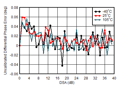
| Differential Phase Error = PhaseOUT(DSA
Setting – 1) – PhaseOUT(DSA Setting) |
Figure 5-132 TX
Uncalibrated Differential Phase Error vs DSA setting and Temperature at 3.5
GHz
| 3.5
GHz Matching, 1TX |
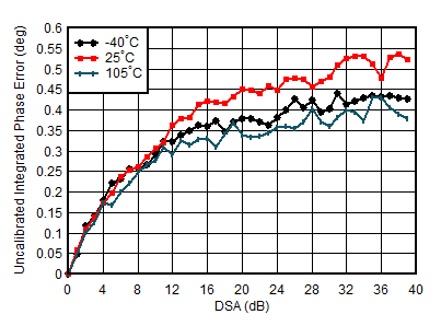
| Integrated Phase Error = Phase(DSA Setting) – Phase(DSA
Setting=0) |
Figure 5-134 TX
Uncalibrated Integrated Phase Error vs DSA Setting and Temperature at 3.5
GHz
A.
| fDAC = 11796.48 MSPS, interleave mode,
matching at 3.5 GHz, Aout = –13 dBFS. |
|
Figure 5-136 TX
NSD vs DSA Setting at 3.5 GHz
| 20-MHz
tone spacing, 3.5 GHz Matching |
|
Figure 5-138 TX
IMD3 vs Digital Amplitude and Channel at 3.5 GHz
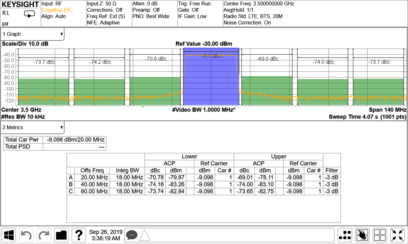
| 3.5
GHz Matching, single carrier 20-MHz BW TM1.1 LTE |
Figure 5-140 TX
20-MHz LTE ACPR vs DSA Setting at 3.5 GHz
| 3.5
GHz Matching, single carrier 20-MHz BW TM1.1 LTE |
Figure 5-142 TX
20-MHz LTE ACPR vs Digital Level at 3.5 GHz
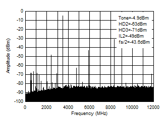
| Matching at 3.5 GHz, fDAC = 11.79648 GSPS,
interleave mode, normalized to output power at harmonic
frequency |
Figure 5-144 TX
Single Tone HD2 vs Frequency and Digital Level at 3.5 GHz
| Matching at 3.5 GHz, fDAC = 11.79648 GSPS,
interleave mode. |
|
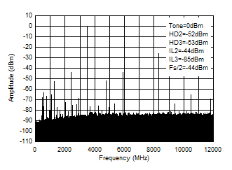
Figure 5-146 TX
Single Tone (–1 dBFS) Output Spectrum at 3.5 GHz (0 -
fDAC)
| Matching at 3.5 GHz, fDAC = 11.79648 GSPS,
interleave mode. |
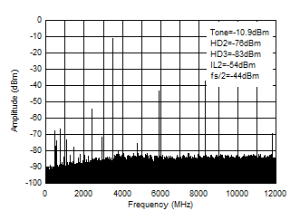
Figure 5-148 TX
Single Tone (–12 dBFS) Output Spectrum at 3.5 GHz
(0-fDAC)
| Aout = -0.5 dFBS, 3.5 GHz Matching,
included PCB and cable losses |
|
Figure 5-119 TX
Output Power vs DSA Setting at 3.5 GHz
| 3.5
GHz Matching, included PCB and cable losses |
| Differential Gain Error = POUT(DSA Setting –
1) – POUT(DSA Setting) + 1 |
Figure 5-121 TX
Calibrated Differential Gain Error vs DSA Setting and Channel at 3.5
GHz
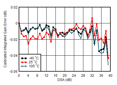
| 3.5
GHz Matching, included PCB and cable losses |
| Integrated Gain Error = POUT(DSA Setting) –
POUT(DSA Setting = 0) + (DSA
Setting) |
Figure 5-123 TX
Calibrated Integrated Gain Error vs DSA Setting and Channel at 3.5
GHz
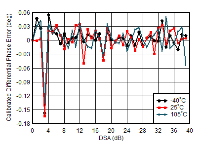
| 3.5
GHz Matching, included PCB and cable losses |
| Phase
DNL spike may occur at any DSA setting. |
Figure 5-125 TX
Calibrated Differential Phase Error vs DSA Setting and Channel at 3.5
GHz
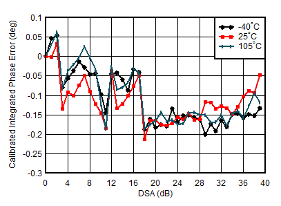
| 3.5
GHz Matching, included PCB and cable losses |
Figure 5-127 TX
Calibrated Integrated Phase Error vs DSA Setting and Channel at 3.5
GHz
| 3.5
GHz Matching, 1TX, Calibrated at 25°C |
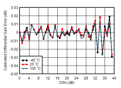
Figure 5-129 TX
Calibrated Differential Gain Error vs DSA Setting and Temperature at 3.5
GHz
| 3.5
GHz Matching, 1TX, Calibrated at 25°C |
|
Figure 5-131 TX
Calibrated Integrated Gain Error vs DSA Setting and Temperature at 3.5
GHz
| 3.5
GHz Matching, 1TX, Calibrated at 25°C |
| Differential Phase Error = PhaseOUT(DSA
Setting – 1) – PhaseOUT(DSA Setting) |
Figure 5-133 TX
Calibrated Differential Phase Error vs DSA Setting and Temperature at 3.5
GHz
| 3.5
GHz Matching, 1TX, Calibrated at 25°C |
| Integrated Phase Error = Phase(DSA Setting) – Phase(DSA
Setting = 0) |
Figure 5-135 TX
Calibrated Integrated Phase Error vs DSA Setting and Temperature at 3.5
GHz
| 20-MHz
tone spacing, 3.5 GHz Matching, –13 dBFS each tone,
included PCB and cable losses |
|
Figure 5-137 TX
IMD3 vs DSA Setting at 3.5 GHz
| 3.5
GHz Matching, single carrier 20-MHz BW TM1.1 LTE |

| 3.5
GHz Matching, single carrier 20-MHz BW TM1.1 LTE |
Figure 5-141 TX
20-MHz LTE alt-ACPR vs DSA Setting at 3.5 GHz
| 3.5
GHz Matching, single carrier 20-MHz BW TM1.1 LTE |
Figure 5-143 TX
20-MHz LTE alt-ACPR vs Digital Level at 3.5 GHz
| Matching at 3.5 GHz, fDAC = 11.79648 GSPS,
interleave mode, normalized to output power at harmonic
frequency. Dip is due to HD3 falling near DC. |
Figure 5-145 TX
Single Tone HD3 vs Frequency and Digital Level at 3.5 GHz
| Matching at 3.5 GHz, fDAC = 11.79648 GSPS,
interleave mode. |
Figure 5-147 TX
Single Tone (–6 dBFS) Output Spectrum at 3.5 GHz (0-fDAC)