AM1802 ARM Microprocessor
1 AM1802 ARM Microprocessor
1.1 Features
- 300-MHzARM926EJ-S™ RISC MPU
- ARM926EJ-S Core
- 32-Bit and 16-Bit (Thumb®) Instructions
- Single-Cycle MAC
- ARM Jazelle® Technology
- Embedded ICE-RT™ for Real-Time Debug
- ARM9™ Memory Architecture
- 16KB of Instruction Cache
- 16KB of Data Cache
- 8KB of RAM (Vector Table)
- 64KB of ROM
- Enhanced Direct Memory Access Controller 3 (EDMA3):
- 2 Channel Controllers
- 3 Transfer Controllers
- 64 Independent DMA Channels
- 16 Quick DMA Channels
- Programmable Transfer Burst Size
- 128KB of On-Chip Memory
- 1.8-V or 3.3-V LVCMOS I/Os (Except for USB and DDR2 Interfaces)
- Two External Memory Interfaces:
- EMIFA
- NOR (8- or 16-Bit-Wide Data)
- NAND (8- or 16-Bit-Wide Data)
- 16-Bit SDRAM with 128-MB Address Space
- DDR2/Mobile DDR Memory Controller with one of the following:
- 16-Bit DDR2 SDRAM with 256-MB Address Space
- 16-Bit mDDR SDRAM with 256-MB Address Space
- Three Configurable 16550-Type UART Modules:
- With Modem Control Signals
- 16-Byte FIFO
- 16x or 13x Oversampling Option
- Two Serial Peripheral Interfaces (SPIs) Each with Multiple Chip Selects
- One Multimedia Card (MMC)/Secure Digital (SD) Card Interfaces with Secure Data I/O (SDIO) Interfaces
- One Master and Slave Inter-Integrated Circuit (I2C Bus™)
- USB 2.0 OTG Port with Integrated PHY (USB0)
- USB 2.0 High- and Full-Speed Client
- USB 2.0 High-, Full-, and Low-Speed Host
- End Point 0 (Control)
- End Points 1, 2, 3, 4 (Control, Bulk, Interrupt or ISOC) RX and TX
- One Multichannel Audio Serial Port (McASP):
- Transmit and Receive Clocks
- Two Clock Zones and 16 Serial Data Pins
- Supports TDM, I2S, and Similar Formats
- DIT-Capable
- FIFO Buffers for Transmit and Receive
- 10/100 Mbps Ethernet MAC (EMAC):
- IEEE 802.3 Compliant
- MII Media-Independent Interface
- RMII Reduced Media-Independent Interface
- Management Data I/O (MDIO) Module
- Real-Time Clock (RTC) with 32-kHz Oscillator and Separate Power Rail
- Three 64-Bit General-Purpose Timers (Each Configurable as Two 32-Bit Timers)
- One 64-Bit General-Purpose or Watchdog Timer (Configurable as Two 32-Bit General-Purpose Timers)
- Packages:
- 361-Ball Pb-Free Plastic Ball Grid Array (PBGA) [ZCE Suffix], 0.65-mm Ball Pitch
- 361-Ball PBGA [ZWT Suffix], 0.80-mm Ball Pitch
- Industrial Temperature
1.2 Applications
- Medical, Healthcare, and Fitness
- Building Automation
- ePOS
1.3 Description
The AM1802 ARM microprocessor is a low-power applications processor based on ARM926EJ-S.
The device enables original-equipment manufacturers (OEMs) and original-design manufacturers (ODMs) to quickly bring to market devices featuring robust operating systems support, rich user interfaces, and high processing performance life through the maximum flexibility of a fully integrated mixed processor solution.
The ARM926EJ-S is a 32-bit RISC processor core that performs 32-bit or 16-bit instructions and processes 32-bit, 16-bit, or 8-bit data. The core uses pipelining so that all parts of the processor and memory system can operate continuously.
The ARM core has a coprocessor 15 (CP15), protection module, and data and program memory management units (MMUs) with table look-aside buffers. The ARM core processor has separate 16-KB instruction and 16-KB data caches. Both are four-way associative with virtual index virtual tag (VIVT). The ARM core also has 8KB of RAM (Vector Table) and 64KB of ROM.
The peripheral set includes: a 10/100 Mbps Ethernet media access controller (EMAC) with a management data input/output (MDIO) module; one USB2.0 OTG interface; one inter-integrated circuit (I2C Bus) interface; one multichannel audio serial port (McASP) with 16 serializers and FIFO buffers; two serial peripheral interfaces (SPIs) with multiple chip selects; four 64-bit general-purpose timers each configurable (one configurable as watchdog); a configurable 16-bit host-port interface (HPI); up to 9 banks of general-purpose input/output (GPIO) pins, with each bank containing 16 pins with programmable interrupt and event generation modes, multiplexed with other peripherals; three UART interfaces (each with RTS and CTS); two external memory interfaces: an asynchronous and SDRAM external memory interface (EMIFA) for slower memories or peripherals; and a higher speed DDR2/Mobile DDR controller.
The EMAC provides an efficient interface between the device and a network. The EMAC supports both 10Base-T and 100Base-TX, or 10 Mbps and 100 Mbps in either half- or full-duplex mode. Additionally, an MDIO interface is available for PHY configuration. The EMAC supports both MII and RMII interfaces.
The rich peripheral set provides the ability to control external peripheral devices and communicate with external processors. For details on each of the peripherals, see the related sections in this document and the associated peripheral reference guides.
The device has a complete set of development tools for the ARM processor. These tools include C compilers, and scheduling, and a Windows® debugger interface for visibility into source code execution.
Device Information
| PART NUMBER | PACKAGE | BODY SIZE |
|---|---|---|
| AM1802ZWT | NFBGA (361) | 16,00 mm x 16,00 mm |
| AM1802ZCE | NFBGA (361) | 13,00 mm x 13,00 mm |
1.4 Functional Block Diagram
Figure 1-1 shows the functional block diagram of the device.
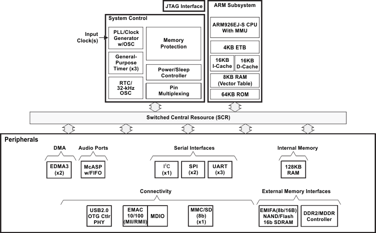 Figure 1-1 Functional Block Diagram
2 Revision History
This data manual revision history highlights the changes made to the SPRS710D device-specific data manual to make it an SPRS710E revision.
Table 2-1 Revision History
| SEE | ADDITIONS/MODIFICATIONS/DELETIONS |
|---|---|
| Global | |
| Section 1.3 Description |
Added NEW Device Information Table. |
| Section 3.7 Terminal Functions |
Table 3-3thruTable 3-18:
|
| Section 3.7.13 Universal Serial Bus Modules (USB0) |
Table 3-15, Universal Serial Bus (USB) Terminal Functions
|
| Section 3.8 Unused Pin Configurations |
Table 3-21, Unused USB0 Signal Configurations:
|
| Section 5 Specifications |
Updated/Changed title from "Device Operating Conditions" to "Specifications" Section 5.2, Handling Ratings:
|
| Section 5.4 Notes on Recommended Power-On Hours |
Table 5-1, Recommended Power-On Hours:
|
| Section 6.10.5 EMIFA Electrical/Timing |
Figure 6-12, Asynchronous Memory Read Timing for EMIFA:
|
| Section 7.1.2 Device and Development-Support Tool Nomenclature |
Figure 7-1, Device Nomenclature:
|
| Section 7.6 Glossary |
Added NEW section. |
3 Device Overview
3.1 Device Characteristics
Table 3-1 provides an overview of the device. The table shows significant features of the device, including the capacity of on-chip RAM, peripherals, and the package type with pin count.
Table 3-1 Characteristics of the Device
| HARDWARE FEATURES | AM1802 | |||
|---|---|---|---|---|
| Peripherals Not all peripherals pins are available at the same time (for more detail, see the Device Configurations section). |
DDR2/mDDR Controller | DDR2, 16-bit bus width, up to 156 MHz Mobile DDR, 16-bit bus width, up to 150 MHz |
||
| EMIFA | Asynchronous (8/16-bit bus width) RAM, Flash, 16-bit SDRAM, NOR, NAND |
|||
| Flash Card Interface | MMC and SD cards supported | |||
| EDMA3 | 64 independent channels, 16 QDMA channels, 2 channel controllers, 3 transfer controllers |
|||
| Timers | 4 64-Bit General Purpose (each configurable as 2 separate 32-bit timers, one configurable as Watch Dog) | |||
| UART | 3 (each with RTS and CTS flow control) | |||
| SPI | 2 (Each with multiple chip selects) | |||
| I2C | 1 (Master/Slave) | |||
| Multichannel Audio Serial Port [McASP] | 1 (each with transmit/receive, FIFO buffer, 16 serializers) | |||
| 10/100 Ethernet MAC with Management Data I/O | 1 (MII or RMII Interface) | |||
| USB 2.0 (USB0) | High-Speed OTG Controller with on-chip OTG PHY | |||
| General-Purpose Input/Output Port | 9 banks of 16-bit | |||
| On-Chip Memory | Size (Bytes) | 168KB RAM | ||
| Organization | ARM 16KB I-Cache 16KB D-Cache 8KB RAM (Vector Table) 64KB ROM ADDITIONAL MEMORY 128KB RAM |
|||
| JTAG BSDL_ID | DEVIDR0 Register | 0x0B7D_102F | ||
| CPU Frequency | MHz | ARM926 300 MHz (1.2V) | ||
| Voltage | Core (V) | 1.2 V nominal for 300 MHz | ||
| I/O (V) | 1.8 V or 3.3 V | |||
| Packages | 13 mm x 13 mm, 361-Ball 0.65 mm pitch, PBGA (ZCE) | |||
| 16 mm x 16 mm, 361-Ball 0.80 mm pitch, PBGA (ZWT) | ||||
| Product Status(1) | Product Preview (PP), Advance Information (AI), or Production Data (PD) |
PD | ||
3.2 Device Compatibility
The ARM926EJ-S RISC CPU is compatible with other ARM9 CPUs from ARM Holdings plc.
3.3 ARM Subsystem
The ARM Subsystem includes the following features:
- ARM926EJ-S RISC processor
- ARMv5TEJ (32/16-bit) instruction set
- Little endian
- System Control Co-Processor 15 (CP15)
- MMU
- 16KB Instruction cache
- 16KB Data cache
- Write Buffer
- Embedded Trace Module and Embedded Trace Buffer (ETM/ETB)
- ARM Interrupt controller
3.3.1 ARM926EJ-S RISC CPU
The ARM Subsystem integrates the ARM926EJ-S processor. The ARM926EJ-S processor is a member of ARM9 family of general-purpose microprocessors. This processor is targeted at multi-tasking applications where full memory management, high performance, low die size, and low power are all important. The ARM926EJ-S processor supports the 32-bit ARM and 16 bit THUMB instruction sets, enabling the user to trade off between high performance and high code density. Specifically, the ARM926EJ-S processor supports the ARMv5TEJ instruction set, which includes features for efficient execution of Java byte codes, providing Java performance similar to Just in Time (JIT) Java interpreter, but without associated code overhead.
The ARM926EJ-S processor supports the ARM debug architecture and includes logic to assist in both hardware and software debug. The ARM926EJ-S processor has a Harvard architecture and provides a complete high performance subsystem, including:
- ARM926EJ -S integer core
- CP15 system control coprocessor
- Memory Management Unit (MMU)
- Separate instruction and data caches
- Write buffer
- Separate instruction and data (internal RAM) interfaces
- Separate instruction and data AHB bus interfaces
- Embedded Trace Module and Embedded Trace Buffer (ETM/ETB)
For more complete details on the ARM9, refer to the ARM926EJ-S Technical Reference Manual, available at http://www.arm.com
3.3.2 CP15
The ARM926EJ-S system control coprocessor (CP15) is used to configure and control instruction and data caches, Memory Management Unit (MMU), and other ARM subsystem functions. The CP15 registers are programmed using the MRC and MCR ARM instructions, when the ARM in a privileged mode such as supervisor or system mode.
3.3.3 MMU
A single set of two level page tables stored in main memory is used to control the address translation, permission checks and memory region attributes for both data and instruction accesses. The MMU uses a single unified Translation Lookaside Buffer (TLB) to cache the information held in the page tables. The MMU features are:
- Standard ARM architecture v4 and v5 MMU mapping sizes, domains and access protection scheme.
- Mapping sizes are:
- 1MB (sections)
- 64KB (large pages)
- 4KB (small pages)
- 1KB (tiny pages)
- Access permissions for large pages and small pages can be specified separately for each quarter of the page (subpage permissions)
- Hardware page table walks
- Invalidate entire TLB, using CP15 register 8
- Invalidate TLB entry, selected by MVA, using CP15 register 8
- Lockdown of TLB entries, using CP15 register 10
3.3.4 Caches and Write Buffer
The size of the Instruction cache is 16KB, Data cache is 16KB. Additionally, the caches have the following features:
- Virtual index, virtual tag, and addressed using the Modified Virtual Address (MVA)
- Four-way set associative, with a cache line length of eight words per line (32-bytes per line) and with two dirty bits in the Dcache
- Dcache supports write-through and write-back (or copy back) cache operation, selected by memory region using the C and B bits in the MMU translation tables
- Critical-word first cache refilling
- Cache lockdown registers enable control over which cache ways are used for allocation on a line fill, providing a mechanism for both lockdown, and controlling cache corruption
- Dcache stores the Physical Address TAG (PA TAG) corresponding to each Dcache entry in the TAG RAM for use during the cache line write-backs, in addition to the Virtual Address TAG stored in the TAG RAM. This means that the MMU is not involved in Dcache write-back operations, removing the possibility of TLB misses related to the write-back address.
- Cache maintenance operations provide efficient invalidation of, the entire Dcache or Icache, regions of the Dcache or Icache, and regions of virtual memory.
The write buffer is used for all writes to a noncachable bufferable region, write-through region and write misses to a write-back region. A separate buffer is incorporated in the Dcache for holding write-back for cache line evictions or cleaning of dirty cache lines. The main write buffer has 16-word data buffer and a four-address buffer. The Dcache write-back has eight data word entries and a single address entry.
3.3.5 Advanced High-Performance Bus (AHB)
The ARM Subsystem uses the AHB port of the ARM926EJ-S to connect the ARM to the Config bus and the external memories. Arbiters are employed to arbitrate access to the separate D-AHB and I-AHB by the Config Bus and the external memories bus.
3.3.6 Embedded Trace Macrocell (ETM) and Embedded Trace Buffer (ETB)
To support real-time trace, the ARM926EJ-S processor provides an interface to enable connection of an Embedded Trace Macrocell (ETM). The ARM926ES-J Subsystem in the device also includes the Embedded Trace Buffer (ETB). The ETM consists of two parts:
- Trace Port provides real-time trace capability for the ARM9.
- Triggering facilities provide trigger resources, which include address and data comparators, counter, and sequencers.
The device trace port is not pinned out and is instead only connected to the Embedded Trace Buffer. The ETB has a 4KB buffer memory. ETB enabled debug tools are required to read/interpret the captured trace data.
3.3.7 ARM Memory Mapping
By default the ARM has access to most on and off chip memory areas, including EMIFA, DDR2, and the additional 128K byte on chip SRAM. Likewise almost all of the on chip peripherals are accessible to the ARM by default.
See Table 3-2 for a detailed top level device memory map that includes the ARM memory space.
3.4 Memory Map Summary
Note: Read/Write accesses to illegal or reserved addresses in the memory map may cause undefined behavior.
Table 3-2 AM1802 Top Level Memory Map
| Start Address | End Address | Size | ARM Mem Map | EDMA Mem Map | Master Peripheral Mem Map |
|---|---|---|---|---|---|
| 0x0000 0000 | 0x01BB FFFF | ||||
| 0x01BC 0000 | 0x01BC 0FFF | 4K | ARM ETB memory | ||
| 0x01BC 1000 | 0x01BC 17FF | 2K | ARM ETB reg | ||
| 0x01BC 1800 | 0x01BC 18FF | 256 | ARM Ice Crusher | ||
| 0x01BC 1900 | 0x01BF FFFF | ||||
| 0x01C0 0000 | 0x01C0 7FFF | 32K | EDMA3 CC | ||
| 0x01C0 8000 | 0x01C0 83FF | 1K | EDMA3 TC0 | ||
| 0x01C0 8400 | 0x01C0 87FF | 1K | EDMA3 TC1 | ||
| 0x01C0 8800 | 0x01C0 FFFF | ||||
| 0x01C1 0000 | 0x01C1 0FFF | 4K | PSC 0 | ||
| 0x01C1 1000 | 0x01C1 1FFF | 4K | PLL Controller 0 | ||
| 0x01C1 2000 | 0x01C1 3FFF | ||||
| 0x01C1 4000 | 0x01C1 4FFF | 4K | SYSCFG0 | ||
| 0x01C1 5000 | 0x01C1 FFFF | ||||
| 0x01C2 0000 | 0x01C2 0FFF | 4K | Timer0 | ||
| 0x01C2 1000 | 0x01C2 1FFF | 4K | Timer1 | ||
| 0x01C2 2000 | 0x01C2 2FFF | 4K | I2C 0 | ||
| 0x01C2 3000 | 0x01C2 3FFF | 4K | RTC | ||
| 0x01C2 4000 | 0x01C3 FFFF | ||||
| 0x01C4 0000 | 0x01C4 0FFF | 4K | MMC/SD 0 | ||
| 0x01C4 1000 | 0x01C4 1FFF | 4K | SPI 0 | ||
| 0x01C4 2000 | 0x01C4 2FFF | 4K | UART 0 | ||
| 0x01C4 3000 | 0x01CF FFFF | ||||
| 0x01D0 0000 | 0x01D0 0FFF | 4K | McASP 0 Control | ||
| 0x01D0 1000 | 0x01D0 1FFF | 4K | McASP 0 AFIFO Ctrl | ||
| 0x01D0 2000 | 0x01D0 2FFF | 4K | McASP 0 Data | ||
| 0x01D0 3000 | 0x01D0 BFFF | ||||
| 0x01D0 C000 | 0x01D0 CFFF | 4K | UART 1 | ||
| 0x01D0 D000 | 0x01D0 DFFF | 4K | UART 2 | ||
| 0x01D0 E000 | 0x01DF FFFF | ||||
| 0x01E0 0000 | 0x01E0 FFFF | 64K | USB0 | ||
| 0x01E1 0000 | 0x01E1 3FFF | ||||
| 0x01E1 4000 | 0x01E1 4FFF | 4K | Memory Protection Unit 1 (MPU 1) | ||
| 0x01E1 5000 | 0x01E1 5FFF | 4K | Memory Protection Unit 2 (MPU 2) | ||
| 0x01E1 6000 | 0x01E1 9FFF | ||||
| 0x01E1 A000 | 0x01E1 AFFF | 4K | PLL Controller 1 | ||
| 0x01E1 B000 | 0x01E1 FFFF | ||||
| 0x01E2 0000 | 0x01E2 1FFF | 8K | EMAC Control Module RAM | ||
| 0x01E2 2000 | 0x01E2 2FFF | 4K | EMAC Control Module Registers | ||
| 0x01E2 3000 | 0x01E2 3FFF | 4K | EMAC Control Registers | ||
| 0x01E2 4000 | 0x01E2 4FFF | 4K | EMAC MDIO port | ||
| 0x01E2 5000 | 0x01E2 5FFF | ||||
| 0x01E2 6000 | 0x01E2 6FFF | 4K | GPIO | ||
| 0x01E2 7000 | 0x01E2 7FFF | 4K | PSC 1 | ||
| 0x01E2 8000 | 0x01E2 BFFF | ||||
| 0x01E2 C000 | 0x01E2 CFFF | 4K | SYSCFG1 | ||
| 0x01E2 D000 | 0x01E2 FFFF | ||||
| 0x01E3 0000 | 0x01E3 7FFF | 32K | EDMA3 CC1 | ||
| 0x01E3 8000 | 0x01E3 83FF | 1K | EDMA3 TC2 | ||
| 0x01E3 8400 | 0x01F0 BFFF | ||||
| 0x01F0 C000 | 0x01F0 CFFF | 4K | Timer2 | ||
| 0x01F0 D000 | 0x01F0 DFFF | 4K | Timer3 | ||
| 0x01F0 E000 | 0x01F0 EFFF | 4K | SPI1 | ||
| 0x01F0 F000 | 0x3FFF FFFF | ||||
| 0x4000 0000 | 0x5FFF FFFF | 512M | EMIFA SDRAM data (CS0) | ||
| 0x6000 0000 | 0x61FF FFFF | 32M | EMIFA async data (CS2) | ||
| 0x6200 0000 | 0x63FF FFFF | 32M | EMIFA async data (CS3) | ||
| 0x6400 0000 | 0x65FF FFFF | 32M | EMIFA async data (CS4) | ||
| 0x6600 0000 | 0x67FF FFFF | 32M | EMIFA async data (CS5) | ||
| 0x6800 0000 | 0x6800 7FFF | 32K | EMIFA Control Regs | ||
| 0x6800 8000 | 0x7FFF FFFF | ||||
| 0x8000 0000 | 0x8001 FFFF | 128K | On-Chip RAM | ||
| 0x8002 0000 | 0xAFFF FFFF | ||||
| 0xB000 0000 | 0xB000 7FFF | 32K | DDR2/mDDR Control Regs | ||
| 0xB000 8000 | 0xBFFF FFFF | ||||
| 0xC000 0000 | 0xCFFF FFFF | 256M | DDR2/mDDR Data | ||
| 0xD000 0000 | 0xE000 0000 | ||||
| 0xFFFD 0000 | 0xFFFD FFFF | 64K | ARM local ROM | ||
| 0xFFFE 0000 | 0xFFFE DFFF | ||||
| 0xFFFE E000 | 0xFFFE FFFF | 8K | ARM Interrupt Controller | ||
| 0xFFFF 0000 | 0xFFFF 1FFF | 8K | ARM local RAM | ||
| 0xFFFF 2000 | 0xFFFF FFFF | ||||
3.5 Pin Assignments
Extensive use of pin multiplexing is used to accommodate the largest number of peripheral functions in the smallest possible package. Pin multiplexing is controlled using a combination of hardware configuration at device reset and software programmable register settings.
3.5.1 Pin Map (Bottom View)
The following graphics show the bottom view of the ZCE and ZWT package pin assignments in four quadrants (A, B, C, and D). The pin assignments for both packages are identical.
 Figure 3-1 Pin Map (Quad A)
 Figure 3-2 Pin Map (Quad B)
 Figure 3-3 Pin Map (Quad C)
 Figure 3-4 Pin Map (Quad D)
3.6 Pin Multiplexing Control
Device level pin multiplexing is controlled by registers PINMUX0 - PINMUX19 in the SYSCFG module.
For the device family, pin multiplexing can be controlled on a pin-by-pin basis. Each pin that is multiplexed with several different functions has a corresponding 4-bit field in one of the PINMUX registers.
Pin multiplexing selects which of several peripheral pin functions controls the pin's IO buffer output data and output enable values only. The default pin multiplexing control for almost every pin is to select 'none' of the peripheral functions in which case the pin's IO buffer is held tri-stated.
Note that the input from each pin is always routed to all of the peripherals that share the pin; the PINMUX registers have no effect on input from a pin.
3.7 Terminal Functions
Table 3-3 to Table 3-20 identify the external signal names, the associated pin/ball numbers along with the mechanical package designator, the pin type (I, O, IO, OZ, or PWR), whether the pin/ball has any internal pullup/pulldown resistors, whether the pin/ball is configurable as an IO in GPIO mode, and a functional pin description.
3.7.1 Device Reset and JTAG
Table 3-3 Reset and JTAG Terminal Functions
| SIGNAL | TYPE(1) | PULL(2) | POWER GROUP(4) |
DESCRIPTION | |
|---|---|---|---|---|---|
| NAME | NO. | ||||
| RESET | |||||
| RESET | K14 | I | IPU | B | Device reset input |
| RESETOUT / GP6[15] | T17 | O(3) | CP[21] | C | Reset output |
| JTAG | |||||
| TMS | L16 | I | IPU | B | JTAG test mode select |
| TDI | M16 | I | IPU | B | JTAG test data input |
| TDO | J18 | O | IPU | B | JTAG test data output |
| TCK | J15 | I | IPU | B | JTAG test clock |
| TRST | L17 | I | IPD | B | JTAG test reset |
| EMU0 | J16 | I/O | IPU | B | Emulation pin |
| EMU1 | K16 | I/O | IPU | B | Emulation pin |
| RTCK/ GP8[0] (5) | K17 | I/O | IPD | B | JTAG Test Clock Return Clock Output General-purpose input/output |
Note: For multiplexed pins where functions have different types (ie., input versus output), the table reflects the pin function direction for that particular peripheral.
3.7.2 High-Frequency Oscillator and PLL
Table 3-4 High-Frequency Oscillator and PLL Terminal Functions
| SIGNAL | TYPE(1) | PULL(2) | POWER GROUP(3) |
DESCRIPTION | |
|---|---|---|---|---|---|
| NAME | NO. | ||||
| CLKOUT / GP6[14] | T18 | O | CP[22] | C | PLL Observation Clock |
| 1.2-V OSCILLATOR | |||||
| OSCIN | L19 | I | — | — | Oscillator input |
| OSCOUT | K19 | O | — | — | Oscillator output |
| OSCVSS | L18 | GND | — | — | Oscillator ground |
| 1.2-V PLL0 | |||||
| PLL0_VDDA | L15 | PWR | — | — | PLL analog VDD (1.2-V filtered supply) |
| PLL0_VSSA | M17 | GND | — | — | PLL analog VSS (for filter) |
| 1.2-V PLL1 | |||||
| PLL1_VDDA | N15 | PWR | — | — | PLL analog VDD (1.2-V filtered supply) |
| PLL1_VSSA | M15 | GND | — | — | PLL analog VSS (for filter) |
Note: For multiplexed pins where functions have different types (ie., input versus output), the table reflects the pin function direction for that particular peripheral.
3.7.3 Real-Time Clock and 32-kHz Oscillator
Table 3-5 Real-Time Clock (RTC) and 1.2-V, 32-kHz Oscillator Terminal Functions
| SIGNAL | TYPE(1) | PULL(2) | POWER GROUP(3) |
DESCRIPTION | |
|---|---|---|---|---|---|
| NAME | NO. | ||||
| RTC_XI | J19 | I | — | — | RTC 32-kHz oscillator input |
| RTC_XO | H19 | O | — | — | RTC 32-kHz oscillator output |
| RTC_ALARM / UART2_CTS / GP0[8] / DEEPSLEEP | F4 | O | CP[0] | A | RTC Alarm |
| RTC_CVDD | L14 | PWR | — | — | RTC module core power (isolated from chip CVDD) |
| RTC_Vss | H18 | GND | — | — | Oscillator ground |
Note: For multiplexed pins where functions have different types (ie., input versus output), the table reflects the pin function direction for that particular peripheral.
3.7.4 DEEPSLEEP Power Control
Table 3-6 DEEPSLEEP Power Control Terminal Functions
| SIGNAL | TYPE(1) | PULL(2) | POWER GROUP(3) |
DESCRIPTION | |
|---|---|---|---|---|---|
| NAME | NO. | ||||
| RTC_ALARM / UART2_CTS / GP0[8] /DEEPSLEEP | F4 | I | CP[0] | A | DEEPSLEEP power control output |
Note: For multiplexed pins where functions have different types (ie., input versus output), the table reflects the pin function direction for that particular peripheral.
3.7.5 External Memory Interface A (EMIFA)
Table 3-7 External Memory Interface A (EMIFA) Terminal Functions
| SIGNAL | TYPE(1) | PULL(2) | POWER GROUP(3) |
DESCRIPTION | |
|---|---|---|---|---|---|
| NAME | NO. | ||||
| EMA_D[15] / GP3[7] | E6 | I/O | CP[17] | B | EMIFA data bus |
| EMA_D[14] / GP3[6] | C7 | I/O | CP[17] | B | |
| EMA_D[13] / GP3[5] | B6 | I/O | CP[17] | B | |
| EMA_D[12] / GP3[4] | A6 | I/O | CP[17] | B | |
| EMA_D[11] / GP3[3] | D6 | I/O | CP[17] | B | |
| EMA_D[10] / GP3[2] | A7 | I/O | CP[17] | B | |
| EMA_D[9] / GP3[1] | D9 | I/O | CP[17] | B | |
| EMA_D[8] / GP3[0] | E10 | I/O | CP[17] | B | |
| EMA_D[7] / GP4[15] | D7 | I/O | CP[17] | B | |
| EMA_D[6] / GP4[14] | C6 | I/O | CP[17] | B | |
| EMA_D[5] / GP4[13] | E7 | I/O | CP[17] | B | |
| EMA_D[4] / GP4[12] | B5 | I/O | CP[17] | B | |
| EMA_D[3] / GP4[11] | E8 | I/O | CP[17] | B | |
| EMA_D[2] / GP4[10] | B8 | I/O | CP[17] | B | |
| EMA_D[1] / GP4[9] | A8 | I/O | CP[17] | B | |
| EMA_D[0] / GP4[8] | C9 | I/O | CP[17] | B | |
| EMA_A[22] / MMCSD0_CMD / GP4[6] | A10 | O | CP[18] | B | EMIFA address bus |
| EMA_A[21] / MMCSD0_DAT[0] / GP4[5] | B10 | O | CP[18] | B | |
| EMA_A[20] / MMCSD0_DAT[1] / GP4[4] | A11 | O | CP[18] | B | |
| EMA_A[19] / MMCSD0_DAT[2] /GP4[3] | C10 | O | CP[18] | B | |
| EMA_A[18] / MMCSD0_DAT[3] / GP4[2] | E11 | O | CP[18] | B | |
| EMA_A[17] / MMCSD0_DAT[4] /GP4[1] | B11 | O | CP[18] | B | |
| EMA_A[16] / MMCSD0_DAT[5] / GP4[0] | E12 | O | CP[18] | B | |
| EMA_A[15] / MMCSD0_DAT[6] / GP5[15] | C11 | O | CP[19] | B | |
| EMA_A[14] / MMCSD0_DAT[7] / GP5[14] | A12 | O | CP[19] | B | |
| EMA_A[13] / GP5[13] | D11 | O | CP[19] | B | |
| EMA_A[12] / GP5[12] | D13 | O | CP[19] | B | |
| EMA_A[11] / GP5[11] | B12 | O | CP[19] | B | |
| EMA_A[10] / GP5[10] | C12 | O | CP[19] | B | |
| EMA_A[9] / GP5[9] | D12 | O | CP[19] | B | |
| EMA_A[8] / GP5[8] | A13 | O | CP[19] | B | |
| EMA_A[7] / GP5[7] | B13 | O | CP[20] | B | |
| EMA_A[6] / GP5[6] | E13 | O | CP[20] | B | |
| EMA_A[5] / GP5[5] | C13 | O | CP[20] | B | |
| EMA_A[4] / GP5[4] | A14 | O | CP[20] | B | |
| EMA_A[3] / GP5[3] | D14 | O | CP[20] | B | |
| EMA_A[2] / GP5[2] | B14 | O | CP[20] | B | |
| EMA_A[1] / GP5[1] | D15 | O | CP[20] | B | |
| EMA_A[0] / GP5[0] | C14 | O | CP[20] | B | |
| EMA_BA[0] / GP2[8] | C15 | O | CP[16] | B | EMIFA bank address |
| EMA_BA[1] / GP2[9] | A15 | O | CP[16] | B | |
| EMA_CLK / GP2[7] | B7 | O | CP[16] | B | EMIFA clock |
| EMA_SDCKE / GP2[6] | D8 | O | CP[16] | B | EMIFA SDRAM clock enable |
| EMA_RAS / GP2[5] | A16 | O | CP[16] | B | EMIFA SDRAM row address strobe |
| EMA_CAS / GP2[4] | A9 | O | CP[16] | B | EMIFA SDRAM column address strobe |
| EMA_CS[0] / GP2[0] | A18 | O | CP[16] | B | EMIFA SDRAM Chip Select |
| EMA_CS[2] / GP3[15] | B17 | O | CP[16] | B | EMIFA Async Chip Select |
| EMA_CS[3] / GP3[14] | A17 | O | CP[16] | B | |
| EMA_CS[4] / GP3[13] | F9 | O | CP[16] | B | |
| EMA_CS[5] / GP3[12] | B16 | O | CP[16] | B | |
| EMA_A_RW / GP3[9] | D10 | O | CP[16] | B | EMIFA Async Read/Write control |
| EMA_WE / GP3[11] | B9 | O | CP[16] | B | EMIFA SDRAM write enable |
| EMA_WEN_DQM[1] / GP2[2] | A5 | O | CP[16] | B | EMIFA write enable/data mask for EMA_D[15:8] |
| EMA_WEN_DQM[0] / GP2[3] | C8 | O | CP[16] | B | EMIFA write enable/data mask for EMA_D[7:0] |
| EMA_OE / GP3[10] | B15 | O | CP[16] | B | EMIFA output enable |
| EMA_WAIT[0] / GP3[8] | B18 | I | CP[16] | B | EMIFA wait input/interrupt |
| EMA_WAIT[1] / GP2[1] | B19 | I | CP[16] | B |
Note: The pin type shown refers to the input, output or high-impedance state of the pin function when configured as the signal name highlighted in bold. All multiplexed signals may enter a high-impedance state when the configured function is input-only or the configured function supports high-Z operation. All GPIO signals can be used as input or output. For multiplexed pins where functions have different types (ie., input versus output), the table reflects the pin function direction for that particular peripheral.
3.7.6 DDR2/mDDR Memory Controller
Table 3-8 DDR2/mDDR Terminal Functions
| SIGNAL | TYPE(1) | PULL(2) | DESCRIPTION | |
|---|---|---|---|---|
| NAME | NO. | |||
| DDR_D[15] | W10 | I/O | IPD | DDR2 SDRAM data bus |
| DDR_D[14] | U11 | I/O | IPD | |
| DDR_D[13] | V10 | I/O | IPD | |
| DDR_D[12] | U10 | I/O | IPD | |
| DDR_D[11] | T12 | I/O | IPD | |
| DDR_D[10] | T10 | I/O | IPD | |
| DDR_D[9] | T11 | I/O | IPD | |
| DDR_D[8] | T13 | I/O | IPD | |
| DDR_D[7] | W11 | I/O | IPD | |
| DDR_D[6] | W12 | I/O | IPD | |
| DDR_D[5] | V12 | I/O | IPD | |
| DDR_D[4] | V13 | I/O | IPD | |
| DDR_D[3] | U13 | I/O | IPD | |
| DDR_D[2] | V14 | I/O | IPD | |
| DDR_D[1] | U14 | I/O | IPD | |
| DDR_D[0] | U15 | I/O | IPD | |
| DDR_A[13] | T5 | O | IPD | DDR2 row/column address |
| DDR_A[12] | V4 | O | IPD | |
| DDR_A[11] | T4 | O | IPD | |
| DDR_A[10] | W4 | O | IPD | |
| DDR_A[9] | T6 | O | IPD | |
| DDR_A[8] | U4 | O | IPD | |
| DDR_A[7] | U6 | O | IPD | |
| DDR_A[6] | W5 | O | IPD | |
| DDR_A[5] | V5 | O | IPD | |
| DDR_A[4] | U5 | O | IPD | |
| DDR_A[3] | V6 | O | IPD | |
| DDR_A[2] | W6 | O | IPD | |
| DDR_A[1] | T7 | O | IPD | |
| DDR_A[0] | U7 | O | IPD | |
| DDR_CLKP | W8 | O | IPD | DDR2 clock (positive) |
| DDR_CLKN | W7 | O | IPD | DDR2 clock (negative) |
| DDR_CKE | V7 | O | IPD | DDR2 clock enable |
| DDR_WE | T8 | O | IPD | DDR2 write enable |
| DDR_RAS | W9 | O | IPD | DDR2 row address strobe |
| DDR_CAS | U9 | O | IPD | DDR2 column address strobe |
| DDR_CS | V9 | O | IPD | DDR2 chip select |
| DDR_DQM[0] | W13 | O | IPD | DDR2 data mask outputs |
| DDR_DQM[1] | R10 | O | IPD | |
| DDR_DQS[0] | T14 | I/O | IPD | DDR2 data strobe inputs/outputs |
| DDR_DQS[1] | V11 | I/O | IPD | |
| DDR_BA[2] | U8 | O | IPD | DDR2 SDRAM bank address |
| DDR_BA[1] | T9 | O | IPD | |
| DDR_BA[0] | V8 | O | IPD | |
| DDR_DQGATE0 | R11 | O | IPD | DDR2 loopback signal for external DQS gating. Route to DDR and back to DDR_DQGATE1 with same constraints as used for DDR clock and data. |
| DDR_DQGATE1 | R12 | I | IPD | DDR2 loopback signal for external DQS gating. Route to DDR and back to DDR_DQGATE0 with same constraints as used for DDR clock and data. |
| DDR_ZP | U12 | O | — | DDR2 reference output for drive strength calibration of N and P channel outputs. Tie to ground via 50 ohm resistor @ 5% tolerance. |
| DDR_VREF | R6 | I | — | DDR voltage input for the DDR2/mDDR I/O buffers. Note even in the case of mDDR an external resistor divider connected to this pin is necessary. |
| DDR_DVDD18 | N10, P10, N9, P9, R9, P8, R8, P7, R7, N6 | PWR | — | DDR PHY 1.8V power supply pins |
Note: The pin type shown refers to the input, output or high-impedance state of the pin function when configured as the signal name highlighted in bold. All multiplexed signals may enter a high-impedance state when the configured function is input-only or the configured function supports high-Z operation. All GPIO signals can be used as input or output. For multiplexed pins where functions have different types (ie., input versus output), the table reflects the pin function direction for that particular peripheral.
3.7.7 Serial Peripheral Interface Modules (SPI)
Table 3-9 Serial Peripheral Interface (SPI) Terminal Functions
| SIGNAL | TYPE(1) | PULL(2) | POWER GROUP(3) |
DESCRIPTION | |
|---|---|---|---|---|---|
| NAME | NO. | ||||
| SPI0 | |||||
| SPI0_CLK / GP1[8] / MII_RXCLK | D19 | I/O | CP[7] | A | SPI0 clock |
| SPI0_ENA / MII_RXDV | C17 | I/O | CP[7] | A | SPI0 enable |
| SPI0_SCS[0] / TM64P1_OUT12 / GP1[6] / MDIO / TM64P1_IN12 | D17 | I/O | CP[10] | A | SPI0 chip selects |
| SPI0_SCS[1] / TM64P0_OUT12 / GP1[7] / MDCLK / TM64P0_IN12 | E16 | I/O | CP[10] | A | |
| SPI0_SCS[2] / UART0_RTS / GP8[1] / MII_RXD[0] | D16 | I/O | CP[9] | A | |
| SPI0_SCS[3] / UART0_CTS / GP8[2] / MII_RXD[1] | E17 | I/O | CP[9] | A | |
| SPI0_SCS[4] / UART0_TXD / GP8[3] / MII_RXD[2] | D18 | I/O | CP[8] | A | |
| SPI0_SCS[5] / UART0_RXD / GP8[4] / MII_RXD[3] | C19 | I/O | CP[8] | A | |
| SPI0_SIMO / GP8[5] / MII_CRS | C18 | I/O | CP[7] | A | SPI0 data slave-in-master-out |
| SPI0_SOMI / GP8[6] / MII_RXER | C16 | I/O | CP[7] | A | SPI0 data slave-out-master-in |
| SPI1 | |||||
| SPI1_CLK / GP2[13] | G19 | I/O | CP[15] | A | SPI1 clock |
| SPI1_ENA / GP2[12] | H16 | I/O | CP[15] | A | SPI1 enable |
| SPI1_SCS[0] /GP2[14] / TM64P3_IN12 | E19 | I/O | CP[14] | A | SPI1 chip selects |
| SPI1_SCS[1] / GP2[15] / TM64P2_IN12 | F18 | I/O | CP[14] | A | |
| SPI1_SCS[2] / UART1_TXD / GP1[0] | F19 | I/O | CP[13] | A | |
| SPI1_SCS[3] / UART1_RXD / GP1[1] | E18 | I/O | CP[13] | A | |
| SPI1_SCS[4] / UART2_TXD / GP1[2] | F16 | I/O | CP[12] | A | |
| SPI1_SCS[5] / UART2_RXD / GP1[3] | F17 | I/O | CP[12] | A | |
| SPI1_SCS[6] / I2C0_SDA / TM64P3_OUT12 / GP1[4] | G18 | I/O | CP[11] | A | |
| SPI1_SCS[7] / I2C0_SCL / TM64P2_OUT12 / GP1[5] | G16 | I/O | CP[11] | A | |
| SPI1_SIMO / GP2[10] | G17 | I/O | CP[15] | A | SPI1 data slave-in-master-out |
| SPI1_SOMI / GP2[11] | H17 | I/O | CP[15] | A | SPI1 data slave-out-master-in |
Note: The pin type shown refers to the input, output or high-impedance state of the pin function when configured as the signal name highlighted in bold. All multiplexed signals may enter a high-impedance state when the configured function is input-only or the configured function supports high-Z operation. All GPIO signals can be used as input or output. For multiplexed pins where functions have different types (ie., input versus output), the table reflects the pin function direction for that particular peripheral.
3.7.8 Boot
Table 3-10 Boot Mode Selection Terminal Functions(3)
| SIGNAL | TYPE(1) | PULL(2) | POWER GROUP(4) |
DESCRIPTION | |
|---|---|---|---|---|---|
| NAME | NO. | ||||
| GP7[7] / BOOT[7] | P4 | I | CP[29] | C | Boot Mode Selection Pins |
| GP7[6] / BOOT[6] | R3 | I | CP[29] | C | |
| GP7[5] / BOOT[5] | R2 | I | CP[29] | C | |
| GP7[4] / BOOT[4] | R1 | I | CP[29] | C | |
| GP7[3] / BOOT[3] | T3 | I | CP[29] | C | |
| GP7[2] / BOOT[2] | T2 | I | CP[29] | C | |
| GP7[1] / BOOT[1] | T1 | I | CP[29] | C | |
| GP7[0] / BOOT[0] | U3 | I | CP[29] | C |
Note: The pin type shown refers to the input, output or high-impedance state of the pin function when configured as the signal name highlighted in bold. All multiplexed signals may enter a high-impedance state when the configured function is input-only or the configured function supports high-Z operation. All GPIO signals can be used as input or output. For multiplexed pins where functions have different types (ie., input versus output), the table reflects the pin function direction for that particular peripheral.
3.7.9 Universal Asynchronous Receiver/Transmitters (UART0, UART1, UART2)
Table 3-11 Universal Asynchronous Receiver/Transmitter (UART) Terminal Functions
| SIGNAL | TYPE(1) | PULL(2) | POWER GROUP(3) |
DESCRIPTION | |
|---|---|---|---|---|---|
| NAME | NO. | ||||
| UART0 | |||||
| SPI0_SCS[5] / UART0_RXD / GP8[4] / MII_RXD[3] | C19 | I | CP[8] | A | UART0 receive data |
| SPI0_SCS[4] / UART0_TXD / GP8[3] / MII_RXD[2] | D18 | O | CP[8] | A | UART0 transmit data |
| SPI0_SCS[2] / UART0_RTS / GP8[1] | D16 | O | CP[9] | A | UART0 ready-to-send output |
| SPI0_SCS[3] / UART0_CTS / GP8[2] | E17 | I | CP[9] | A | UART0 clear-to-send input |
| UART1 | |||||
| SPI1_SCS[3] / UART1_RXD / GP1[1] | E18 | I | CP[13] | A | UART1 receive data |
| SPI1_SCS[2] / UART1_TXD / GP1[0] | F19 | O | CP[13] | A | UART1 transmit data |
| AHCLKR / UART1_RTS / GP0[11] | A2 | O | CP[0] | A | UART1 ready-to-send output |
| AHCLKX / USB_REFCLKIN / UART1_CTS / GP0[10] | A3 | I | CP[0] | A | UART1 clear-to-send input |
| UART2 | |||||
| SPI1_SCS[5] / UART2_RXD / GP1[3] | F17 | I | CP[12] | A | UART2 receive data |
| SPI1_SCS[4] / UART2_TXD / GP1[2] | F16 | O | CP[12] | A | UART2 transmit data |
| AMUTE / UART2_RTS / GP0[9] | D5 | O | CP[0] | A | UART2 ready-to-send output |
| RTC_ALARM / UART2_CTS / GP0[8] / DEEPSLEEP | F4 | I | CP[0] | A | UART2 clear-to-send input |
Note: The pin type shown refers to the input, output or high-impedance state of the pin function when configured as the signal name highlighted in bold. All multiplexed signals may enter a high-impedance state when the configured function is input-only or the configured function supports high-Z operation. All GPIO signals can be used as input or output. For multiplexed pins where functions have different types (ie., input versus output), the table reflects the pin function direction for that particular peripheral.
3.7.10 Inter-Integrated Circuit Modules (I2C0)
Table 3-12 Inter-Integrated Circuit (I2C) Terminal Functions
| SIGNAL | TYPE(1) | PULL(2) | POWER GROUP(3) |
DESCRIPTION | |
|---|---|---|---|---|---|
| NAME | NO. | ||||
| I2C0 | |||||
| SPI1_SCS[6] / I2C0_SDA / TM64P3_OUT12 / GP1[4] | G18 | I/O | CP[11] | A | I2C0 serial data |
| SPI1_SCS[7] / I2C0_SCL / TM64P2_OUT12 / GP1[5] | G16 | I/O | CP[11] | A | I2C0 serial clock |
Note: The pin type shown refers to the input, output or high-impedance state of the pin function when configured as the signal name highlighted in bold. All multiplexed signals may enter a high-impedance state when the configured function is input-only or the configured function supports high-Z operation. All GPIO signals can be used as input or output. For multiplexed pins where functions have different types (ie., input versus output), the table reflects the pin function direction for that particular peripheral.
3.7.11 Timers
Table 3-13 Timers Terminal Functions
| SIGNAL | TYPE(1) | PULL(2) | POWER GROUP(3) |
DESCRIPTION | ||
|---|---|---|---|---|---|---|
| NAME | NO. | |||||
| TIMER0 | ||||||
| SPI0_SCS[1] / TM64P0_OUT12 / GP1[7] / MDCLK / TM64P0_IN12 | E16 | I | CP[10] | A | Timer0 lower input | |
| SPI0_SCS[1] / TM64P0_OUT12 / GP1[7] / MDCLK / TM64P0_IN12 | E16 | O | CP[10] | A | Timer0 lower output | |
| TIMER1 (Watchdog) | ||||||
| SPI0_SCS[0] / TM64P1_OUT12 / GP1[6] / MDIO / TM64P1_IN12 | D17 | I | CP[10] | A | Timer1 lower input | |
| SPI0_SCS[0] / TM64P1_OUT12 / GP1[6] / MDIO /TM64P1_IN12 | D17 | O | CP[10] | A | Timer1 lower output | |
| TIMER2 | ||||||
| SPI1_SCS[1] / GP2[15] / TM64P2_IN12 | F18 | I | CP[14] | A | Timer2 lower input | |
| SPI1_SCS[7] / I2C0_SCL / TM64P2_OUT12 / GP1[5] | G16 | O | CP[11] | A | Timer2 lower output | |
| TIMER3 | ||||||
| SPI1_SCS[0] / GP2[14] / TM64P3_IN12 | E19 | I | CP[14] | A | Timer3 lower input | |
| SPI1_SCS[6] / I2C0_SDA / TM64P3_OUT12 / GP1[4] | G18 | O | CP[11] | A | Timer3 lower output | |
Note: The pin type shown refers to the input, output or high-impedance state of the pin function when configured as the signal name highlighted in bold. All multiplexed signals may enter a high-impedance state when the configured function is input-only or the configured function supports high-Z operation. All GPIO signals can be used as input or output. For multiplexed pins where functions have different types (ie., input versus output), the table reflects the pin function direction for that particular peripheral.
3.7.12 Multichannel Audio Serial Ports (McASP)
Table 3-14 Multichannel Audio Serial Ports Terminal Functions
| SIGNAL | TYPE(1) | PULL(2) | POWER GROUP(3) |
DESCRIPTION | ||
|---|---|---|---|---|---|---|
| NAME | NO. | |||||
| McASP0 | ||||||
| AXR15 / GP0[7] | A4 | I/O | CP[1] | A | McASP0 serial data | |
| AXR14 / GP0[6] | B4 | I/O | CP[2] | A | ||
| AXR13 / GP0[5] | B3 | I/O | CP[2] | A | ||
| AXR12 / GP0[4] | C4 | I/O | CP[2] | A | ||
| AXR11 / GP0[3] | C5 | I/O | CP[2] | A | ||
| AXR10 / GP0[2] | D4 | I/O | CP[2] | A | ||
| AXR9 / GP0[1] | C3 | I/O | CP[2] | A | ||
| AXR8 / GP0[0] | E4 | I/O | CP[3] | A | ||
| AXR7 / GP1[15] | D2 | I/O | CP[4] | A | ||
| AXR6 / GP1[14] / MII_TXEN | C1 | I/O | CP[5] | A | ||
| AXR5 / GP1[13] / MII_TXCLK | D3 | I/O | CP[5] | A | ||
| AXR4 / GP1[12] / MII_COL | D1 | I/O | CP[5] | A | ||
| AXR3 / GP1[11] / MII_TXD[3] | E3 | I/O | CP[5] | A | ||
| AXR2 / GP1[10] / MII_TXD[2] | E2 | I/O | CP[5] | A | ||
| AXR1 / GP1[9] / MII_TXD[1] | E1 | I/O | CP[5] | A | ||
| AXR0 / GP8[7] / MII_TXD[0] | F3 | I/O | CP[6] | A | ||
| AHCLKX / USB_REFCLKIN / UART1_CTS / GP0[10] | A3 | I/O | CP[0] | A | McASP0 transmit master clock | |
| ACLKX / GP0[14] | B1 | I/O | CP[0] | A | McASP0 transmit bit clock | |
| AFSX / GP0[12] | B2 | I/O | CP[0] | A | McASP0 transmit frame sync | |
| AHCLKR / UART1_RTS /GP0[11] | A2 | I/O | CP[0] | A | McASP0 receive master clock | |
| ACLKR / GP0[15] | A1 | I/O | CP[0] | A | McASP0 receive bit clock | |
| AFSR / GP0[13] | C2 | I/O | CP[0] | A | McASP0 receive frame sync | |
| AMUTE / UART2_RTS / GP0[9] | D5 | I/O | CP[0] | A | McASP0 mute output | |
Note: The pin type shown refers to the input, output or high-impedance state of the pin function when configured as the signal name highlighted in bold. All multiplexed signals may enter a high-impedance state when the configured function is input-only or the configured function supports high-Z operation. All GPIO signals can be used as input or output. For multiplexed pins where functions have different types (ie., input versus output), the table reflects the pin function direction for that particular peripheral.
3.7.13 Universal Serial Bus Modules (USB0)
Table 3-15 Universal Serial Bus (USB) Terminal Functions
| SIGNAL | TYPE(1) | PULL(2) | POWER GROUP(3) |
DESCRIPTION | |
|---|---|---|---|---|---|
| NAME | NO. | ||||
| USB0 2.0 OTG (USB0) | |||||
| USB0_DM | M18 | A | IPD | — | USB0 PHY data minus |
| USB0_DP | M19 | A | IPD | — | USB0 PHY data plus |
| USB0_VDDA33 | N18 | PWR | — | — | USB0 PHY 3.3-V supply |
| USB0_ID | P16 | A | — | — | USB0 PHY identification (mini-A or mini-B plug) |
| USB0_VBUS | N19 | A | — | — | USB0 bus voltage |
| USB0_DRVVBUS | K18 | O | IPD | B | USB0 controller VBUS control output. |
| AHCLKX / USB_REFCLKIN / UART1_CTS / GP0[10] | A3 | I | CP[0] | A | USB_REFCLKIN. Optional clock input |
| USB0_VDDA18 | N14 | PWR | — | — | USB0 PHY 1.8-V supply input |
| USB0_VDDA12 | N17 | A | — | — | USB0 PHY 1.2-V LDO output for bypass cap For proper device operation, this pin must always be connected via a 0.22-μF capacitor to VSS (GND), even if USB0 is not being used. |
| USB_CVDD | M12 | PWR | — | — | USB0 core logic 1.2-V supply input |
Note: The pin type shown refers to the input, output or high-impedance state of the pin function when configured as the signal name highlighted in bold. All multiplexed signals may enter a high-impedance state when the configured function is input-only or the configured function supports high-Z operation. All GPIO signals can be used as input or output. For multiplexed pins where functions have different types (ie., input versus output), the table reflects the pin function direction for that particular peripheral.
3.7.14 Ethernet Media Access Controller (EMAC)
Table 3-16 Ethernet Media Access Controller (EMAC) Terminal Functions
| SIGNAL | TYPE(1) | PULL(2) | POWER GROUP(3) |
DESCRIPTION | |
|---|---|---|---|---|---|
| NAME | NO. | ||||
| MII | |||||
| AXR6 / GP1[14] / MII_TXEN | C1 | O | CP[5] | A | EMAC MII Transmit enable output |
| AXR5 / GP1[13] / MII_TXCLK | D3 | I | CP[5] | A | EMAC MII Transmit clock input |
| AXR4 / GP1[12] / MII_COL | D1 | I | CP[5] | A | EMAC MII Collision detect input |
| AXR3 / GP1[11] / MII_TXD[3] | E3 | O | CP[5] | A | EMAC MII transmit data |
| AXR2 / GP1[10] / MII_TXD[2] | E2 | O | CP[5] | A | |
| AXR1 / GP1[9] / MII_TXD[1] | E1 | O | CP[5] | A | |
| AXR0 / GP8[7] / MII_TXD[0] | F3 | O | CP[6] | A | |
| SPI0_SOMI / GP8[6] / MII_RXER | C16 | I | CP[7] | A | EMAC MII receive error input |
| SPI0_SIMO / GP8[5] / MII_CRS | C18 | I | CP[7] | A | EMAC MII carrier sense input |
| SPI0_CLK / GP1[8] / MII_RXCLK | D19 | I | CP[7] | A | EMAC MII receive clock input |
| SPI0_ENA / MII_RXDV | C17 | I | CP[7] | A | EMAC MII receive data valid input |
| SPI0_SCS[5] / UART0_RXD / GP8[4] / MII_RXD[3] | C19 | I | CP[8] | A | EMAC MII receive data |
| SPI0_SCS[4] / UART0_TXD / GP8[3] / MII_RXD[2] | D18 | I | CP[8] | A | |
| SPI0_SCS[3] / UART0_CTS / GP8[2] / MII_RXD[1] | E17 | I | CP[9] | A | |
| SPI0_SCS[2] / UART0_RTS / GP8[1] / MII_RXD[0] | D16 | I | CP[9] | A | |
| RMII | |||||
| RMII_MHZ_50_CLK | W18 | I/O | CP[26] | C | EMAC 50-MHz clock input or output |
| RMII_RXER | W17 | I | CP[26] | C | EMAC RMII receiver error |
| RMII_RXD[0] | V17 | I | CP[26] | C | EMAC RMII receive data |
| RMII_RXD[1] | W16 | I | CP[26] | C | |
| RMII_CRS_DV | W19 | I | CP[26] | C | EMAC RMII carrier sense data valid |
| RMII_TXEN | R14 | O | CP[26] | C | EMAC RMII transmit enable |
| RMII_TXD[0] | V16 | O | CP[26] | C | EMAC RMII transmit data |
| RMII_TXD[1] | U18 | O | CP[26] | C | |
| MDIO | |||||
| SPI0_SCS[0] / TM64P1_OUT12 / GP1[6] / MDIO / TM64P1_IN12 | D17 | I/O | CP[10] | A | MDIO serial data |
| SPI0_SCS[1] / TM64P0_OUT12 / GP1[7] / MDCLK / TM64P0_IN12 | E16 | O | CP[10] | A | MDIO clock |
Note: The pin type shown refers to the input, output or high-impedance state of the pin function when configured as the signal name highlighted in bold. All multiplexed signals may enter a high-impedance state when the configured function is input-only or the configured function supports high-Z operation. All GPIO signals can be used as input or output. For multiplexed pins where functions have different types (ie., input versus output), the table reflects the pin function direction for that particular peripheral.
3.7.15 Multimedia Card/Secure Digital (MMC/SD)
Table 3-17 Multimedia Card/Secure Digital (MMC/SD) Terminal Functions
| SIGNAL | TYPE(1) | PULL(2) | POWER GROUP(3) |
DESCRIPTION | |
|---|---|---|---|---|---|
| NAME | NO. | ||||
| MMCSD0 | |||||
| MMCSD0_CLK / GP4[7] | E9 | O | CP[18] | B | MMCSD0 Clock |
| EMA_A[22] / MMCSD0_CMD / GP4[6] | A10 | I/O | CP[18] | B | MMCSD0 Command |
| EMA_A[14] / MMCSD0_DAT[7] / GP5[14] | A12 | I/O | CP[19] | B | MMC/SD0 data |
| EMA_A[15] / MMCSD0_DAT[6] / GP5[15] | C11 | I/O | CP[19] | B | |
| EMA_A[16] / MMCSD0_DAT[5] / GP4[0] | E12 | I/O | CP[18] | B | |
| EMA_A[17] / MMCSD0_DAT[4] / GP4[1] | B11 | I/O | CP[18] | B | |
| EMA_A[18] / MMCSD0_DAT[3] / GP4[2] | E11 | I/O | CP[18] | B | |
| EMA_A[19] / MMCSD0_DAT[2] / GP4[3] | C10 | I/O | CP[18] | B | |
| EMA_A[20] / MMCSD0_DAT[1] / GP4[4] | A11 | I/O | CP[18] | B | |
| EMA_A[21] / MMCSD0_DAT[0] / GP4[5] | B10 | I/O | CP[18] | B | |
Note: The pin type shown refers to the input, output or high-impedance state of the pin function when configured as the signal name highlighted in bold. All multiplexed signals may enter a high-impedance state when the configured function is input-only or the configured function supports high-Z operation. All GPIO signals can be used as input or output. For multiplexed pins where functions have different types (ie., input versus output), the table reflects the pin function direction for that particular peripheral.
3.7.16 General Purpose Input Output
Table 3-18 General Purpose Input Output Terminal Functions
| SIGNAL | TYPE(1) | PULL(2) | POWER GROUP(3) |
DESCRIPTION | |
|---|---|---|---|---|---|
| NAME | NO. | ||||
| GP0 | |||||
| ACLKR / GP0[15] | A1 | I/O | CP[0] | A | GPIO Bank 0 |
| ACLKX / GP0[14] | B1 | I/O | CP[0] | A | |
| AFSR / GP0[13] | C2 | I/O | CP[0] | A | |
| AFSX / GP0[12] | B2 | I/O | CP[0] | A | |
| AHCLKR / UART1_RTS / GP0[11] | A2 | I/O | CP[0] | A | |
| AHCLKX / USB_REFCLKIN / UART1_CTS / GP0[10] | A3 | I/O | CP[0] | A | |
| AMUTE / UART2_RTS / GP0[9] | D5 | I/O | CP[0] | A | |
| RTC_ALARM / UART2_CTS / GP0[8] / DEEPSLEEP | F4 | I/O | CP[0] | A | |
| AXR15 / GP0[7] | A4 | I/O | CP[1] | A | |
| AXR14 / GP0[6] | B4 | I/O | CP[2] | A | |
| AXR13 / GP0[5] | B3 | I/O | CP[2] | A | |
| AXR12 / GP0[4] | C4 | I/O | CP[2] | A | |
| AXR11 / GP0[3] | C5 | I/O | CP[2] | A | |
| AXR10 / GP0[2] | D4 | I/O | CP[2] | A | |
| AXR9 / GP0[1] | C3 | I/O | CP[2] | A | |
| AXR8 / GP0[0] | E4 | I/O | CP[3] | A | |
| GP1 | |||||
| AXR7 / GP1[15] | D2 | I/O | CP[4] | A | GPIO Bank 1 |
| AXR6 / GP1[14] / MII_TXEN | C1 | I/O | CP[5] | A | |
| AXR5 / GP1[13] / MII_TXCLK | D3 | I/O | CP[5] | A | |
| AXR4 / GP1[12] / MII_COL | D1 | I/O | CP[5] | A | |
| AXR3 / GP1[11] / MII_TXD[3] | E3 | I/O | CP[5] | A | |
| AXR2 / GP1[10] / MII_TXD[2] | E2 | I/O | CP[5] | A | |
| AXR1 / GP1[9] / MII_TXD[1] | E1 | I/O | CP[5] | A | |
| SPI0_CLK / GP1[8] / MII_RXCLK | D19 | I/O | CP[7] | A | |
| SPI0_SCS[1] / TM64P0_OUT12 / GP1[7] / MDCLK / TM64P0_IN12 | E16 | I/O | CP[10] | A | |
| SPI0_SCS[0] / TM64P1_OUT12 / GP1[6] / MDIO / TM64P1_IN12 | D17 | I/O | CP[10] | A | |
| SPI1_SCS[7] / I2C0_SCL / TM64P2_OUT12 / GP1[5] | G16 | I/O | CP[11] | A | |
| SPI1_SCS[6] / I2C0_SDA / TM64P3_OUT12 / GP1[4] | G18 | I/O | CP[11] | A | |
| SPI1_SCS[5] / UART2_RXD / GP1[3] | F17 | I/O | CP[12] | A | |
| SPI1_SCS[4] / UART2_TXD / GP1[2] | F16 | I/O | CP[12] | A | |
| SPI1_SCS[3] / UART1_RXD / GP1[1] | E18 | I/O | CP[13] | A | |
| SPI1_SCS[2] / UART1_TXD / GP1[0] | F19 | I/O | CP[13] | A | |
| GP2 | |||||
| SPI1_SCS[1] / GP2[15] / TM64P2_IN12 | F18 | I/O | CP[14] | A | GPIO Bank 2 |
| SPI1_SCS[0] / GP2[14] / TM64P3_IN12 | E19 | I/O | CP[14] | A | |
| SPI1_CLK / GP2[13] | G19 | I/O | CP[15] | A | |
| SPI1_ENA / GP2[12] | H16 | I/O | CP[15] | A | |
| SPI1_SOMI / GP2[11] | H17 | I/O | CP[15] | A | |
| SPI1_SIMO / GP2[10] | G17 | I/O | CP[15] | A | |
| EMA_BA[1] / GP2[9] | A15 | I/O | CP[16] | B | |
| EMA_BA[0] / GP2[8] | C15 | I/O | CP[16] | B | |
| EMA_CLK / GP2[7] | B7 | I/O | CP[16] | B | |
| EMA_SDCKE / GP2[6] | D8 | I/O | CP[16] | B | |
| EMA_RAS / GP2[5] | A16 | I/O | CP[16] | B | |
| EMA_CAS / GP2[4] | A9 | I/O | CP[16] | B | |
| EMA_WEN_DQM[0] / GP2[3] | C8 | I/O | CP[16] | B | |
| EMA_WEN_DQM[1] / GP2[2] | A5 | I/O | CP[16] | B | |
| EMA_WAIT[1] / GP2[1] | B19 | I/O | CP[16] | B | |
| EMA_CS[0] / GP2[0] | A18 | I/O | CP[16] | B | |
| GP3 | |||||
| EMA_CS[2] / GP3[15] | B17 | I/O | CP[16] | B | GPIO Bank 3 |
| EMA_CS[3] / GP3[14] | A17 | I/O | CP[16] | B | |
| EMA_CS[4] / GP3[13] | F9 | I/O | CP[16] | B | |
| EMA_CS[5] / GP3[12] | B16 | I/O | CP[16] | B | |
| EMA_WE / GP3[11] | B9 | I/O | CP[16] | B | |
| EMA_OE / GP3[10] | B15 | I/O | CP[16] | B | |
| EMA_A_RW / GP3[9] | D10 | I/O | CP[16] | B | |
| EMA_WAIT[0] / GP3[8] | B18 | I/O | CP[16] | B | |
| EMA_D[15] / GP3[7] | E6 | I/O | CP[17] | B | |
| EMA_D[14] / GP3[6] | C7 | I/O | CP[17] | B | |
| EMA_D[13] / GP3[5] | B6 | I/O | CP[17] | B | |
| EMA_D[12] / GP3[4] | A6 | I/O | CP[17] | B | |
| EMA_D[11] / GP3[3] | D6 | I/O | CP[17] | B | |
| EMA_D[10] / GP3[2] | A7 | I/O | CP[17] | B | |
| EMA_D[9] / GP3[1] | D9 | I/O | CP[17] | B | |
| EMA_D[8] / GP3[0] | E10 | I/O | CP[17] | B | |
| GP4 | |||||
| EMA_D[7] / GP4[15] | D7 | I/O | CP[17] | B | GPIO Bank 4 |
| EMA_D[6] / GP4[14] | C6 | I/O | CP[17] | B | |
| EMA_D[5] / GP4[13] | E7 | I/O | CP[17] | B | |
| EMA_D[4] / GP4[12] | B5 | I/O | CP[17] | B | |
| EMA_D[3] / GP4[11] | E8 | I/O | CP[17] | B | |
| EMA_D[2] / GP4[10] | B8 | I/O | CP[17] | B | |
| EMA_D[1] / GP4[9] | A8 | I/O | CP[17] | B | |
| EMA_D[0] / GP4[8] | C9 | I/O | CP[17] | B | |
| MMCSD0_CLK / GP4[7] | E9 | I/O | CP[18] | B | |
| EMA_A[22] / MMCSD0_CMD / GP4[6] | A10 | I/O | CP[18] | B | |
| EMA_A[21] / MMCSD0_DAT[0] / GP4[5] | B10 | I/O | CP[18] | B | |
| EMA_A[20] / MMCSD0_DAT[1] / GP4[4] | A11 | I/O | CP[18] | B | |
| EMA_A[19] / MMCSD0_DAT[2] / GP4[3] | C10 | I/O | CP[18] | B | |
| EMA_A[18] / MMCSD0_DAT[3] / GP4[2] | E11 | I/O | CP[18] | B | |
| EMA_A[17] / MMCSD0_DAT[4] / GP4[1] | B11 | I/O | CP[18] | B | |
| EMA_A[16] / MMCSD0_DAT[5] / GP4[0] | E12 | I/O | CP[18] | B | |
| GP5 | |||||
| EMA_A[15] / MMCSD0_DAT[6] / GP5[15] | C11 | I/O | CP[19] | B | GPIO Bank 5 |
| EMA_A[14] / MMCSD0_DAT[7] / GP5[14] | A12 | I/O | CP[19] | B | |
| EMA_A[13] / GP5[13] | D11 | I/O | CP[19] | B | |
| EMA_A[12] / GP5[12] | D13 | I/O | CP[19] | B | |
| EMA_A[11] / GP5[11] | B12 | I/O | CP[19] | B | |
| EMA_A[10] / GP5[10] | C12 | I/O | CP[19] | B | |
| EMA_A[9] / GP5[9] | D12 | I/O | CP[19] | B | |
| EMA_A[8] / GP5[8] | A13 | I/O | CP[19] | B | |
| EMA_A[7] / GP5[7] | B13 | I/O | CP[20] | B | |
| EMA_A[6] / GP5[6] | E13 | I/O | CP[20] | B | |
| EMA_A[5] / GP5[5] | C13 | I/O | CP[20] | B | |
| EMA_A[4] / GP5[4] | A14 | I/O | CP[20] | B | |
| EMA_A[3] / GP5[3] | D14 | I/O | CP[20] | B | |
| EMA_A[2] / GP5[2] | B14 | I/O | CP[20] | B | |
| EMA_A[1] / GP5[1] | D15 | I/O | CP[20] | B | |
| EMA_A[0] / GP5[0] | C14 | I/O | CP[20] | B | |
| GP6 | |||||
| RESETOUT / GP6[15] | T17 | I/O | CP[21] | C | GPIO Bank 6 |
| CLKOUT / GP6[14] | T18 | I/O | CP[22] | C | |
| GP6[13] | R17 | I/O | CP[23] | C | |
| GP6[12] | R16 | I/O | CP[23] | C | |
| GP6[11] | U17 | I/O | CP[24] | C | |
| GP6[10] | W15 | I/O | CP[24] | C | |
| GP6[9] | U16 | I/O | CP[24] | C | |
| GP6[8] | T15 | I/O | CP[24] | C | |
| GP6[7] | W14 | I/O | CP[25] | C | |
| GP6[6] | V15 | I/O | CP[25] | C | |
| GP6[5] | P17 | I/O | CP[27] | C | |
| GP6[4] | H3 | I/O | CP[30] | C | |
| GP6[3] | K3 | I/O | CP[30] | C | |
| GP6[2] | J3 | I/O | CP[30] | C | |
| GP6[1] | K4 | I/O | CP[30] | C | |
| GP6[0] | R5 | I/O | CP[31] | C | |
| GP7 | |||||
| GP7[15] | U2 | I/O | CP[28] | C | GPIO Bank 7 |
| GP7[14] | U1 | I/O | CP[28] | C | |
| GP7[13] | V3 | I/O | CP[28] | C | |
| GP7[12] | V2 | I/O | CP[28] | C | |
| GP7[11] | V1 | I/O | CP[28] | C | |
| GP7[10] | W3 | I/O | CP[28] | C | |
| GP7[9] | W2 | I/O | CP[28] | C | |
| GP7[8] | W1 | I/O | CP[28] | C | |
| GP7[7] / BOOT[7] | P4 | I/O | CP[29] | C | |
| GP7[6] / BOOT[6] | R3 | I/O | CP[29] | C | |
| GP7[5] / BOOT[5] | R2 | I/O | CP[29] | C | |
| GP7[4] / BOOT[4] | R1 | I/O | CP[29] | C | |
| GP7[3] / BOOT[3] | T3 | I/O | CP[29] | C | |
| GP7[2] / BOOT[2] | T2 | I/O | CP[29] | C | |
| GP7[1] / BOOT[1] | T1 | I/O | CP[29] | C | |
| GP7[0] / BOOT[0] | U3 | I/O | CP[29] | C | |
| GP8 | |||||
| GP8[15] | G1 | I/O | CP30] | C | GPIO Bank 8 |
| GP8[14] | G2 | I/O | CP[30] | C | |
| GP8[13] | J4 | I/O | CP[30] | C | |
| GP8[12] | G3 | I/O | CP[30] | C | |
| GP8[11] | F1 | I/O | CP[31] | C | |
| GP8[10] | F2 | I/O | CP[31] | C | |
| GP8[9] | H4 | I/O | CP[31] | C | |
| GP8[8] | G4 | I/O | CP[31] | C | |
| AXR0 / GP8[7] / MII_TXD[0] | F3 | I/O | CP[6] | A | |
| SPI0_SOMI / GP8[6] / MII_RXER | C16 | I/O | CP[7] | A | |
| SPI0_SIMO / GP8[5] / MII_CR | C18 | I/O | CP[7] | A | |
| SPI0_SCS[5] / UART0_RXD / GP8[4] / MII_RXD[3] | C19 | I/O | CP[8] | A | |
| SPI0_SCS[4] / UART0_TXD / GP8[3] / MII_RXD[2] | D18 | I/O | CP[8] | A | |
| SPI0_SCS[3] / UART0_CTS / GP8[2] / MII_RXD[1] | E17 | I/O | CP[9] | A | |
| SPI0_SCS[2] / UART0_RTS / GP8[1] / MII_RXD[0] | D16 | I/O | CP[9] | A | |
| RTCK / GP8[0](5) | K17 | I/O | IPD | B | |
Note: The pin type shown refers to the input, output or high-impedance state of the pin function when configured as the signal name highlighted in bold. All multiplexed signals may enter a high-impedance state when the configured function is input-only or the configured function supports high-Z operation. All GPIO signals can be used as input or output. For multiplexed pins where functions have different types (ie., input versus output), the table reflects the pin function direction for that particular peripheral.
3.7.17 Reserved and No Connect
Table 3-19 Reserved and No Connect Terminal Functions
| SIGNAL | TYPE(1) | DESCRIPTION | |
|---|---|---|---|
| NAME | NO. | ||
| RSV2 | T19 | PWR | Reserved. For proper device operation, this pin must be tied either directly to CVDD or left unconnected (do not connect to ground). |
| NC_J1 | J1 | — | These signals should be left unconnected (do not connect to connect to power or ground). |
| NC_J2 | J2 | — | |
| NC_L1 | L1 | — | |
| NC_L2 | L2 | — | |
| NC_M2 | M2 | — | |
| NC_M3 | M3 | — | |
| NC_M14 | M14 | — | |
| NC_N1 | N1 | — | |
| NC_N2 | N2 | — | |
| NC_N3 | N3 | — | |
| NC_N4 | N4 | — | |
| NC_N16 | N16 | — | |
| NC_P1 | P1 | — | |
| NC_P2 | P2 | — | |
| NC_P3 | P3 | — | |
| NC_P14 | P14 | — | |
| NC_P15 | P15 | — | |
| NC_P18 | P18 | — | |
| NC_P19 | P19 | — | |
| NC_R15 | R15 | — | |
| NC_R18 | R18 | — | |
| NC_R19 | R19 | — | |
| NC_T16 | T16 | — | |
| NC_U19 | U19 | — | |
| NC_V18 | V18 | — | |
| NC_V19 | V19 | — | |
| RSVDN | J17 | I | Reserved. For proper device operation, the pin must be pulled up to supply DVDD3318_B. |
3.7.18 Supply and Ground
Table 3-20 Supply and Ground Terminal Functions
| SIGNAL | TYPE(1) | DESCRIPTION | |
|---|---|---|---|
| NAME | NO. | ||
| CVDD (Core supply) | E15, G7, G8, G13, H6, H7, H10, H11, H12, H13, J6, J12, K6, K12, L12, M8, M9, N8 | PWR | Variable (1.2V - 1.0V) core supply voltage pins |
| RVDD (Internal RAM supply) | E5, H14, N7 | PWR | 1.2V internal ram supply voltage pins |
| DVDD18 (I/O supply) | F14, G6, G10, G11, G12, J13, K5, L6, P13, R13 | PWR | 1.8V I/O supply voltage pins. DVDD18 must be powered even if all of the DVDD3318_x supplies are operated at 3.3V. |
| DVDD3318_A (I/O supply) | F5, F15, G5, G14, G15, H5 | PWR | 1.8V or 3.3-V dual-voltage LVCMOS I/O supply voltage pins, Group A |
| DVDD3318_B (I/O supply) | E14, F6, F7, F8, F10, F11, F12, F13, G9, J14, K15 | PWR | 1.8V or 3.3-V dual-voltage LVCMOS I/O supply voltage pins, Group B |
| DVDD3318_C (I/O supply) | J5, K13, L4, L13, M13, N13, P5, P6, P12, R4 | PWR | 1.8V or 3.3-V dual-voltage LVCMOS I/O supply voltage pins, Group C |
| VSS (Ground) | A19, H1, H2, H8, H9, H15, J7, J8, J9, J10, J11, K1, K2, K7, K8, K9, K10, K11, L3, L5, L7, L8, L9, L10, L11, M1, M4, M5, M6, M7, M10, M11, N5, N11, N12, P11 | GND | Ground pins. |
| USB0_VDDA33 | N18 | PWR | USB0 PHY 3.3-V supply |
| USB0_VDDA18 | N14 | PWR | USB0 PHY 1.8-V supply input |
| USB0_VDDA12 | N17 | A | USB0 PHY 1.2-V LDO output for bypass cap |
| USB_CVDD | M12 | PWR | USB0 core logic 1.2-V supply input |
| DDR_DVDD18 | N10, P10, N9, P9, R9, P8, R8, P7, R7, N6 | PWR | DDR PHY 1.8V power supply pins |
3.8 Unused Pin Configurations
All signals multiplexed with multiple functions may be used as an alternate function if a given peripheral is not used. Unused non-multiplexed signals and some other specific signals should be handled as specified in the tables below.
Table 3-21 Unused USB0 Signal Configurations
| SIGNAL NAME | Configuration (When USB0 is not used) |
|---|---|
| USB0_DM | No Connect |
| USB0_DP | No Connect |
| USB0_ID | No Connect |
| USB0_VBUS | No Connect |
| USB0_DRVVBUS | No Connect |
| USB0_VDDA33 | No Connect |
| USB0_VDDA18 | No Connect |
| USB0_VDDA12 | Internal USB PHY output connected to an external 0.22-μF filter capacitor |
| USB_REFCLKIN | No Connect or other peripheral function |
| USB_CVDD | 1.2V |
Table 3-22 Unused RTC Signal Configuration
| SIGNAL NAME | Configuration |
|---|---|
| RTC_XI | May be held high (CVDD) or low |
| RTC_XO | No Connect |
| RTC_ALARM | May be used as GPIO or other peripheral function |
| RTC_CVDD | Connect to CVDD |
| RTC_VSS | VSS |
Table 3-23 Unused DDR2/mDDR Controller Signal Configuration
| SIGNAL NAME | Configuration (1) |
|---|---|
| DDR_D[15:0] | No Connect |
| DDR_A[13:0] | No Connect |
| DDR_CLKP | No Connect |
| DDR_CLKN | No Connect |
| DDR_CKE | No Connect |
| DDR_WE | No Connect |
| DDR_RAS | No Connect |
| DDR_CAS | No Connect |
| DDS_CS | No Connect |
| DDR_DQM[1:0] | No Connect |
| DDR_DQS[1:0] | No Connect |
| DDR_BA[2:0] | No Connect |
| DDR_DQGATE0 | No Connect |
| DDR_DQGATE1 | No Connect |
| DDR_ZP | No Connect |
| DDR_VREF | No Connect |
| DDR_DVDD18 | No Connect |
4 Device Configuration
4.1 Boot Modes
This device supports a variety of boot modes through an internal ARM ROM bootloader. This device does not support dedicated hardware boot modes. The input states of the BOOT pins are sampled and latched into the BOOTCFG register, which is part of the system configuration (SYSCFG) module, when device reset is deasserted. Boot mode selection is determined by the values of the BOOT pins.
See Using the OMAP-L1x8 Bootloader Application Report (SPRAB41) for more details on the ROM Boot Loader.
The following boot modes are supported:
- NAND Flash boot
- 8-bit NAND
- 16-bit NAND (supported on ROM revisions after d800k002 -- see the bootloader documents mentioned above to determine the ROM revision)
- NOR Flash boot
- NOR Direct boot (8-bit or 16-bit)
- NOR Legacy boot (8-bit or 16-bit)
- NOR AIS boot (8-bit or 16-bit)
- I2C0 Boot
- EEPROM (Master Mode)
- External Host (Slave Mode)
- SPI0/ SPI1 Boot
- Serial Flash (Master Mode)
- SERIAL EEPROM (Master Mode)
- External Host (Slave Mode)
- UART0/UART1/UART2 Boot
- External Host
- MMC/SD0 Boot
4.2 SYSCFG Module
The following system level features of the chip are controlled by the SYSCFG peripheral:
- Readable Device, Die, and Chip Revision ID
- Control of Pin Multiplexing
- Priority of bus accesses different bus masters in the system
- Capture at power on reset the chip BOOT pin values and make them available to software
- Control of the DeepSleep power management function
- Enable and selection of the programmable pin pullups and pulldowns
- Special case settings for peripherals:
- Locking of PLL controller settings
- Default burst sizes for EDMA3 transfer controllers
- McASP AMUTEIN selection and clearing of AMUTE status for the McASP
- Control of the reference clock source and other side-band signals for both of the integrated USB PHYs
- Clock source selection for EMIFA
- DDR2 Controller PHY settings
- Selects the source of emulation suspend signal (from ARM) of peripherals supporting this function.
Many registers are accessible only by a host (ARM) when it is operating in its privileged mode. (ex. from the kernel, but not from user space code).
Table 4-1 System Configuration (SYSCFG) Module Register Access
| Register Address | Register Name | Register Description | Register Access |
|---|---|---|---|
| 0x01C1 4000 | REVID | Revision Identification Register | — |
| 0x01C14008 | DIEIDR0 | Device Identification Register 0 | — |
| 0x01C1400C | DIEIDR1 | Device Identification Register 1 | — |
| 0x01C14010 | DIEIDR2 | Device Identification Register 2 | — |
| 0x01C14014 | DIEIDR3 | Device Identification Register 3 | — |
| 0x01C1 4020 | BOOTCFG | Boot Configuration Register | Privileged mode |
| 0x01C1 4038 | KICK0R | Kick 0 Register | Privileged mode |
| 0x01C1 403C | KICK1R | Kick 1 Register | Privileged mode |
| 0x01C1 4040 | HOST0CFG | Host 0 Configuration Register | — |
| 0x01C1 4044 | HOST1CFG | Host 1 Configuration Register | — |
| 0x01C1 40E0 | IRAWSTAT | Interrupt Raw Status/Set Register | Privileged mode |
| 0x01C1 40E4 | IENSTAT | Interrupt Enable Status/Clear Register | Privileged mode |
| 0x01C1 40E8 | IENSET | Interrupt Enable Register | Privileged mode |
| 0x01C1 40EC | IENCLR | Interrupt Enable Clear Register | Privileged mode |
| 0x01C1 40F0 | EOI | End of Interrupt Register | Privileged mode |
| 0x01C1 40F4 | FLTADDRR | Fault Address Register | Privileged mode |
| 0x01C1 40F8 | FLTSTAT | Fault Status Register | — |
| 0x01C1 4110 | MSTPRI0 | Master Priority 0 Registers | Privileged mode |
| 0x01C1 4114 | MSTPRI1 | Master Priority 1 Registers | Privileged mode |
| 0x01C1 4118 | MSTPRI2 | Master Priority 2 Registers | Privileged mode |
| 0x01C1 4120 | PINMUX0 | Pin Multiplexing Control 0 Register | Privileged mode |
| 0x01C1 4124 | PINMUX1 | Pin Multiplexing Control 1 Register | Privileged mode |
| 0x01C1 4128 | PINMUX2 | Pin Multiplexing Control 2 Register | Privileged mode |
| 0x01C1 412C | PINMUX3 | Pin Multiplexing Control 3 Register | Privileged mode |
| 0x01C1 4130 | PINMUX4 | Pin Multiplexing Control 4 Register | Privileged mode |
| 0x01C1 4134 | PINMUX5 | Pin Multiplexing Control 5 Register | Privileged mode |
| 0x01C1 4138 | PINMUX6 | Pin Multiplexing Control 6 Register | Privileged mode |
| 0x01C1 413C | PINMUX7 | Pin Multiplexing Control 7 Register | Privileged mode |
| 0x01C1 4140 | PINMUX8 | Pin Multiplexing Control 8 Register | Privileged mode |
| 0x01C1 4144 | PINMUX9 | Pin Multiplexing Control 9 Register | Privileged mode |
| 0x01C1 4148 | PINMUX10 | Pin Multiplexing Control 10 Register | Privileged mode |
| 0x01C1 414C | PINMUX11 | Pin Multiplexing Control 11 Register | Privileged mode |
| 0x01C1 4150 | PINMUX12 | Pin Multiplexing Control 12 Register | Privileged mode |
| 0x01C1 4154 | PINMUX13 | Pin Multiplexing Control 13 Register | Privileged mode |
| 0x01C1 4158 | PINMUX14 | Pin Multiplexing Control 14 Register | Privileged mode |
| 0x01C1 415C | PINMUX15 | Pin Multiplexing Control 15 Register | Privileged mode |
| 0x01C1 4160 | PINMUX16 | Pin Multiplexing Control 16 Register | Privileged mode |
| 0x01C1 4164 | PINMUX17 | Pin Multiplexing Control 17 Register | Privileged mode |
| 0x01C1 4168 | PINMUX18 | Pin Multiplexing Control 18 Register | Privileged mode |
| 0x01C1 416C | PINMUX19 | Pin Multiplexing Control 19 Register | Privileged mode |
| 0x01C1 4170 | SUSPSRC | Suspend Source Register | Privileged mode |
| 0x01C1 4174 | Reserved | — | |
| 0x01C1 4178 | Reserved | — | |
| 0x01C1 417C | CFGCHIP0 | Chip Configuration 0 Register | Privileged mode |
| 0x01C1 4180 | CFGCHIP1 | Chip Configuration 1 Register | Privileged mode |
| 0x01C1 4184 | CFGCHIP2 | Chip Configuration 2 Register | Privileged mode |
| 0x01C1 4188 | CFGCHIP3 | Chip Configuration 3 Register | Privileged mode |
| 0x01C1 418C | CFGCHIP4 | Chip Configuration 4 Register | Privileged mode |
| 0x01E2 C000 | VTPIO_CTL | VTPIO COntrol Register | Privileged mode |
| 0x01E2 C004 | DDR_SLEW | DDR Slew Register | Privileged mode |
| 0x01E2 C008 | DeepSleep | DeepSleep Register | Privileged mode |
| 0x01E2 C00C | PUPD_ENA | Pullup / Pulldown Enable Register | Privileged mode |
| 0x01E2 C010 | PUPD_SEL | Pullup / Pulldown Selection Register | Privileged mode |
| 0x01E2 C014 | RXACTIVE | RXACTIVE Control Register | Privileged mode |
| 0x01E2 C018 | PWRDN | PWRDN Control Register | Privileged mode |
4.3 Pullup/Pulldown Resistors
Proper board design should ensure that input pins to the device always be at a valid logic level and not floating. This may be achieved via pullup/pulldown resistors. The device features internal pullup (IPU) and internal pulldown (IPD) resistors on most pins to eliminate the need, unless otherwise noted, for external pullup/pulldown resistors.
An external pullup/pulldown resistor needs to be used in the following situations:
- Boot and Configuration Pins: If the pin is both routed out and 3-stated (not driven), an external pullup/pulldown resistor is strongly recommended, even if the IPU/IPD matches the desired value/state.
- Other Input Pins: If the IPU/IPD does not match the desired value/state, use an external pullup/pulldown resistor to pull the signal to the opposite rail.
For the boot and configuration pins, if they are both routed out and 3-stated (not driven), it is strongly recommended that an external pullup/pulldown resistor be implemented. Although, internal pullup/pulldown resistors exist on these pins and they may match the desired configuration value, providing external connectivity can help ensure that valid logic levels are latched on these device boot and configuration pins. In addition, applying external pullup/pulldown resistors on the boot and configuration pins adds convenience to the user in debugging and flexibility in switching operating modes.
Tips for choosing an external pullup/pulldown resistor:
- Consider the total amount of current that may pass through the pullup or pulldown resistor. Make sure to include the leakage currents of all the devices connected to the net, as well as any internal pullup or pulldown resistors.
- Decide a target value for the net. For a pulldown resistor, this should be below the lowest VIL level of all inputs connected to the net. For a pullup resistor, this should be above the highest VIH level of all inputs on the net. A reasonable choice would be to target the VOL or VOH levels for the logic family of the limiting device; which, by definition, have margin to the VIL and VIH levels.
- Select a pullup/pulldown resistor with the largest possible value; but, which can still ensure that the net will reach the target pulled value when maximum current from all devices on the net is flowing through the resistor. The current to be considered includes leakage current plus, any other internal and external pullup/pulldown resistors on the net.
- For bidirectional nets, there is an additional consideration which sets a lower limit on the resistance value of the external resistor. Verify that the resistance is small enough that the weakest output buffer can drive the net to the opposite logic level (including margin).
- Remember to include tolerances when selecting the resistor value.
- For pullup resistors, also remember to include tolerances on the IO supply rail.
- For most systems, a 1-kΩ resistor can be used to oppose the IPU/IPD while meeting the above criteria. Users should confirm this resistor value is correct for their specific application.
- For most systems, a 20-kΩ resistor can be used to compliment the IPU/IPD on the boot and configuration pins while meeting the above criteria. Users should confirm this resistor value is correct for their specific application.
- For more detailed information on input current (II), and the low-/high-level input voltages (VIL and VIH) for the device, see Section 5.3, Recommended Operating Conditions.
- For the internal pullup/pulldown resistors for all device pins, see the peripheral/system-specific terminal functions table.