SPRSP65G April 2021 – May 2024 AM2431 , AM2432 , AM2434
PRODUCTION DATA
- 1
- 1 Features
- 2 Applications
- 3 Description
- 4 Device Comparison
-
5 Terminal Configuration and Functions
- 5.1 Pin Diagram
- 5.2 Pin Attributes
- 5.3
Signal Descriptions
- 17
- 5.3.1 AM243x_ALX Package - Unsupported Interfaces and Signals
- 5.3.2 ADC
- 5.3.3 CPSW
- 5.3.4 CPTS
- 5.3.5 DDRSS
- 5.3.6 ECAP
- 5.3.7 Emulation and Debug
- 5.3.8 EPWM
- 5.3.9 EQEP
- 5.3.10 FSI
- 5.3.11 GPIO
- 5.3.12 GPMC
- 5.3.13 I2C
- 5.3.14 MCAN
- 5.3.15 SPI (MCSPI)
- 5.3.16 MMC
- 5.3.17 OSPI
- 5.3.18 Power Supply
- 5.3.19 PRU_ICSSG
- 5.3.20 Reserved
- 5.3.21 SERDES
- 5.3.22 System and Miscellaneous
- 5.3.23 TIMER
- 5.3.24 UART
- 5.3.25 USB
- 5.4 Pin Connectivity Requirements
-
6 Specifications
- 6.1 Absolute Maximum Ratings
- 6.2 ESD Ratings
- 6.3 Power-On Hours (POH)
- 6.4 Recommended Operating Conditions
- 6.5 Operating Performance Points
- 6.6 Power Consumption Summary
- 6.7
Electrical Characteristics
- 6.7.1 I2C Open-Drain, and Fail-Safe (I2C OD FS) Electrical Characteristics
- 6.7.2 Fail-Safe Reset (FS RESET) Electrical Characteristics
- 6.7.3 High-Frequency Oscillator (HFOSC) Electrical Characteristics
- 6.7.4 eMMCPHY Electrical Characteristics
- 6.7.5 SDIO Electrical Characteristics
- 6.7.6 LVCMOS Electrical Characteristics
- 6.7.7 ADC12B Electrical Characteristics (ALV package)
- 6.7.8 ADC10B Electrical Characteristics (ALX package)
- 6.7.9 USB2PHY Electrical Characteristics
- 6.7.10 SerDes PHY Electrical Characteristics
- 6.7.11 DDR Electrical Characteristics
- 6.8 VPP Specifications for One-Time Programmable (OTP) eFuses
- 6.9 Thermal Resistance Characteristics
- 6.10
Timing and Switching Characteristics
- 6.10.1 Timing Parameters and Information
- 6.10.2 Power Supply Requirements
- 6.10.3 System Timing
- 6.10.4 Clock Specifications
- 6.10.5
Peripherals
- 6.10.5.1 CPSW3G
- 6.10.5.2 DDRSS
- 6.10.5.3 ECAP
- 6.10.5.4 EPWM
- 6.10.5.5 EQEP
- 6.10.5.6 FSI
- 6.10.5.7 GPIO
- 6.10.5.8 GPMC
- 6.10.5.9 I2C
- 6.10.5.10 MCAN
- 6.10.5.11 MCSPI
- 6.10.5.12 MMCSD
- 6.10.5.13 CPTS
- 6.10.5.14 OSPI
- 6.10.5.15 PCIe
- 6.10.5.16
PRU_ICSSG
- 6.10.5.16.1 PRU_ICSSG Programmable Real-Time Unit (PRU)
- 6.10.5.16.2 PRU_ICSSG Pulse Width Modulation (PWM)
- 6.10.5.16.3 PRU_ICSSG Industrial Ethernet Peripheral (IEP)
- 6.10.5.16.4 PRU_ICSSG Universal Asynchronous Receiver Transmitter (UART)
- 6.10.5.16.5 PRU_ICSSG Enhanced Capture Peripheral (ECAP)
- 6.10.5.16.6 PRU_ICSSG RGMII, MII_RT, and Switch
- 6.10.5.17 Timers
- 6.10.5.18 UART
- 6.10.5.19 USB
- 6.10.6 Emulation and Debug
-
7 Detailed Description
- 7.1 Overview
- 7.2 Processor Subsystems
- 7.3 Accelerators and Coprocessors
- 7.4
Other Subsystems
- 7.4.1 PDMA Controller
- 7.4.2
Peripherals
- 7.4.2.1 ADC
- 7.4.2.2 DCC
- 7.4.2.3 Dual Date Rate (DDR) External Memory Interface (DDRSS)
- 7.4.2.4 ECAP
- 7.4.2.5 EPWM
- 7.4.2.6 ELM
- 7.4.2.7 ESM
- 7.4.2.8 GPIO
- 7.4.2.9 EQEP
- 7.4.2.10 General-Purpose Memory Controller (GPMC)
- 7.4.2.11 I2C
- 7.4.2.12 MCAN
- 7.4.2.13 MCRC Controller
- 7.4.2.14 MCSPI
- 7.4.2.15 MMCSD
- 7.4.2.16 OSPI
- 7.4.2.17 Peripheral Component Interconnect Express (PCIe)
- 7.4.2.18 Serializer/Deserializer (SerDes) PHY
- 7.4.2.19 Real Time Interrupt (RTI/WWDT)
- 7.4.2.20 Dual Mode Timer (DMTIMER)
- 7.4.2.21 UART
- 7.4.2.22 Universal Serial Bus Subsystem (USBSS)
-
8 Applications,
Implementation, and Layout
- 8.1 Device Connection and Layout Fundamentals
- 8.2
Peripheral- and Interface-Specific Design Information
- 8.2.1 General Routing Guidelines
- 8.2.2 DDR Board Design and Layout Guidelines
- 8.2.3 OSPI/QSPI/SPI Board Design and Layout Guidelines
- 8.2.4 USB VBUS Design Guidelines
- 8.2.5 System Power Supply Monitor Design Guidelines
- 8.2.6 High Speed Differential Signal Routing Guidance
- 8.2.7 Thermal Solution Guidance
- 8.3 Clock Routing Guidelines
- 9 Device and Documentation Support
- 10Revision History
- 11Mechanical, Packaging, and Orderable Information
Package Options
Refer to the PDF data sheet for device specific package drawings
Mechanical Data (Package|Pins)
- ALV|441
- ALX|293
Thermal pad, mechanical data (Package|Pins)
Orderable Information
6.10.4.1.1.2 Shunt Capacitance
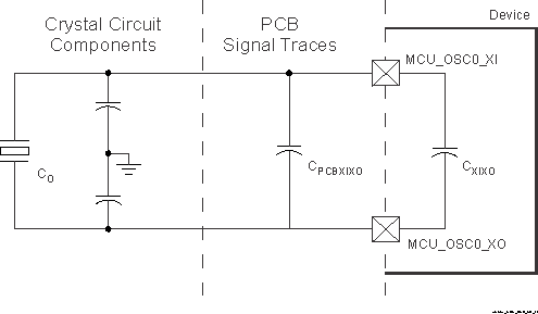
The crystal circuit must also be designed such that it does not exceed the maximum shunt capacitance for MCU_OSC0 operating conditions defined in Table 6-19. Shunt capacitance, Cshunt, of the crystal circuit is a combination of crystal shunt capacitance and parasitic contributions. PCB signal traces which connect crystal circuit components to MCU_OSC0 have mutual parasitic capacitance to each other, CPCBXIXO, where the PCB designer should be able to extract mutual parasitic capacitance between these signal traces. The device package also has mutual parasitic capacitance, CXIXO, where this mutual parasitic capacitance value is defined in Table 6-20.
PCB routing should be designed to minimize mutual capacitance between XI and XO signal traces. This is typically done by keeping signal traces short and not routing them in close proximity. Mutual capacitance can also be minimized by placing a ground trace between these signals when the layout requires them to be routed in close proximity. It is important to minimize the mutual capacitance on the PCB to provide as much margin as possible when selecting a crystal.
 Figure 6-18 Shunt Capacitance
A crystal should be chosen such that the below equation is satisfied. CO in the equation is the maximum shunt capacitance specified by the crystal manufacturer.
Cshunt ≥ CO + CPCBXIXO + CXIXO
For example, the equation would be satisfied when the crystal being used is 25MHz with an ESR = 30 Ω, CPCBXIXO = 0.04 pF, CXIXO = 0.01 pF, and shunt capacitance of the crystal is less than or equal to 6.95 pF.