SLLS104M December   1990  – October 2023 AM26C32 , AM26C32C , AM26C32M

PRODUCTION DATA  

  1.   1
  2. Features
  3. Applications
  4. Description
  5. Pin Configuration and Functions
  6. Specifications
    1. 5.1 Absolute Maximum Ratings
    2. 5.2 ESD Ratings
    3. 5.3 Recommended Operating Conditions
    4. 5.4 Thermal Information
    5. 5.5 Thermal Information
    6. 5.6 Electrical Characteristics
    7. 5.7 Switching Characteristics
    8. 5.8 Typical Characteristics
  7. Parameter Measurement Information
  8. Detailed Description
    1. 7.1 Overview
    2. 7.2 Functional Block Diagram
    3. 7.3 Feature Description
      1. 7.3.1 ±7-V Common-Mode Range With ±200-mV Sensitivity
      2. 7.3.2 Input Fail-Safe Circuitry
      3. 7.3.3 Active-High and Active-Low
      4. 7.3.4 Operates from a Single 5-V Supply
    4. 7.4 Device Functional Modes
      1. 7.4.1 Enable and Disable
  9. Application and Implementation
    1. 8.1 Application Information
    2. 8.2 Typical Application
      1. 8.2.1 Design Requirements
      2. 8.2.2 Detailed Design Procedure
      3. 8.2.3 Application Curve
    3. 8.3 Power Supply Recommendations
    4. 8.4 Layout
      1. 8.4.1 Layout Guidelines
      2. 8.4.2 Layout Example
  10. Device and Documentation Support
    1. 9.1 Receiving Notification of Documentation Updates
    2. 9.2 Support Resources
    3. 9.3 Trademarks
    4. 9.4 Electrostatic Discharge Caution
    5. 9.5 Glossary
  11. 10Revision History
  12. 11Mechanical, Packaging, and Orderable Information

Package Options

Refer to the PDF data sheet for device specific package drawings

Mechanical Data (Package|Pins)
  • DB|16
  • PW|16
  • NS|16
  • N|16
  • D|16
Thermal pad, mechanical data (Package|Pins)
Orderable Information

Parameter Measurement Information

GUID-9C217396-A036-4264-8771-8A7B2B5D46C8-low.gif
CL includes probe and jig capacitance.
Figure 6-1 Switching Test Circuit and Voltage Waveforms
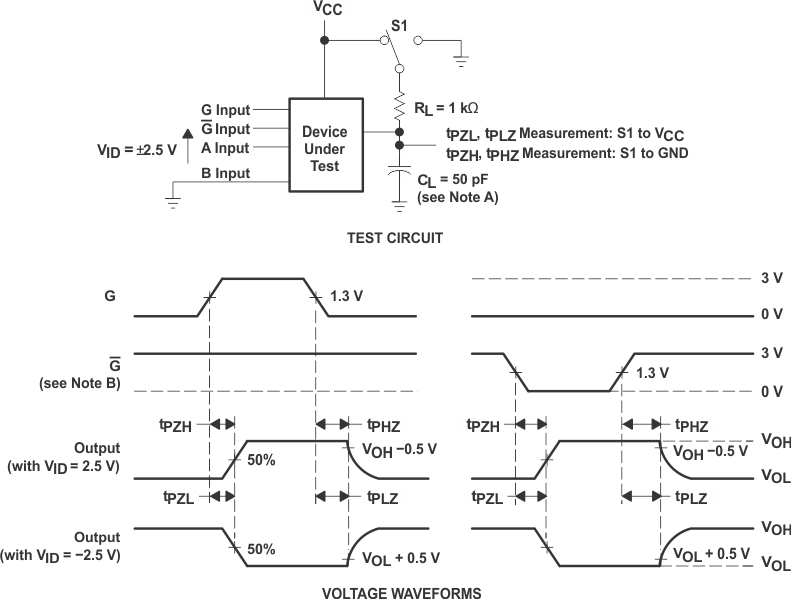
GUID-481CE8D5-810B-421C-BECA-A5C3459761D5-low.gif
CL includes probe and jig capacitance.
The input pulse is supplied by a generator having the following characteristics: PRR = 1 MHz, duty cycle ≤ 50%, tr = tf = 6 ns.
Figure 6-2 Enable/Disable Time Test Circuit and Output Voltage Waveforms