SLLS202H may   1995  – august 2023 AM26LV32

PRODUCTION DATA  

  1.   1
  2. Features
  3. Applications
  4. Description
  5. Revision History
  6. Pin Configuration and Functions
  7. Specifications
    1. 6.1 Absolute Maximum Ratings
    2. 6.2 ESD Ratings
    3. 6.3 Recommended Operating Conditions
    4. 6.4 Thermal Information
    5. 6.5 Electrical Characteristics
    6. 6.6 Switching Characteristics
    7. 6.7 Typical Characteristics
  8. Parameter Measurement Information
  9. Detailed Description
    1. 8.1 Overview
    2. 8.2 Functional Block Diagram
    3. 8.3 Feature Description
    4. 8.4 Device Functional Modes
      1. 8.4.1 Fail-Safe Conditions
      2. 8.4.2 Fail-Safe Precautions
  10. Application and Implementation
    1. 9.1 Application Information
    2. 9.2 Typical Application
      1. 9.2.1 Design Requirements
      2. 9.2.2 Detailed Design Procedure
      3. 9.2.3 Application Curve
    3. 9.3 Power Supply Recommendations
    4. 9.4 Layout
      1. 9.4.1 Layout Guidelines
      2. 9.4.2 Layout Example
  11. 10Device and Documentation Support
    1. 10.1 Receiving Notification of Documentation Updates
    2. 10.2 Support Resources
    3. 10.3 Trademarks
    4. 10.4 Electrostatic Discharge Caution
    5. 10.5 Glossary
  12. 11Mechanical, Packaging, and Orderable Information

Package Options

Refer to the PDF data sheet for device specific package drawings

Mechanical Data (Package|Pins)
  • NS|16
  • D|16
Thermal pad, mechanical data (Package|Pins)
Orderable Information

Typical Characteristics

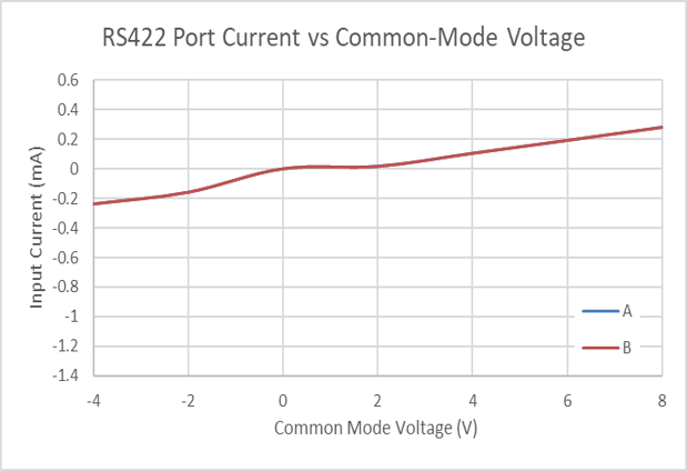
GUID-20230801-SS0I-RSZK-XNBS-BCMSQ6KMJ493-low.pngFigure 6-1 RS422 Port Current vs Common-Mode Voltage
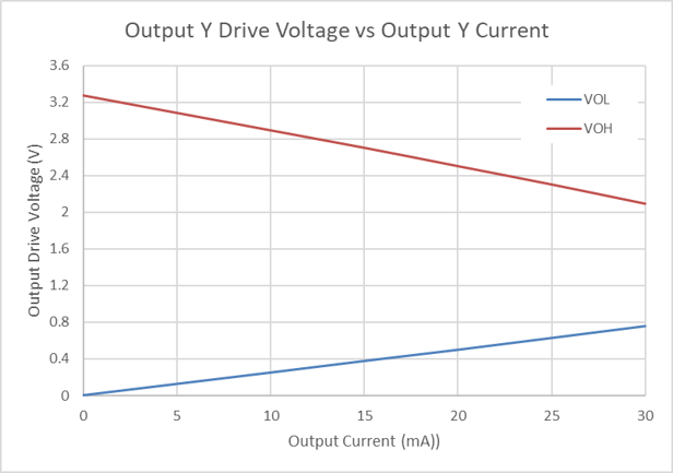
GUID-20230801-SS0I-2N8Z-VC1L-L8GL9DXKBBR7-low.pngFigure 6-3 Output Y Drive Voltage vs Output Y Current
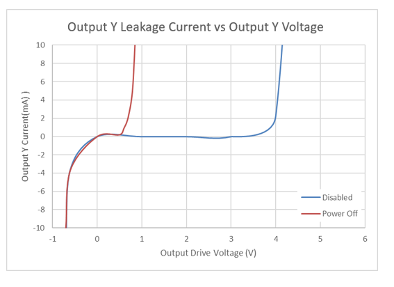
GUID-20230801-SS0I-MSGX-G2LG-4QJTQGGFTDKZ-low.pngFigure 6-2 Output Y Leakage Current vs Output Y Voltage