SPRSP98A November   2023  – June 2024 AM625SIP

PRODUCTION DATA  

  1.   1
  2. Features
  3. Applications
  4. Description
    1. 3.1 Functional Block Diagram
  5. Device Comparison
    1. 4.1 Related Products
  6. Terminal Configuration and Functions
    1. 5.1 Pin Diagrams
    2. 5.2 Pin Attributes and Signal Descriptions
  7. Specifications
    1. 6.1 Absolute Maximum Ratings
    2. 6.2 ESD Ratings
    3. 6.3 Recommended Operating Conditions
    4. 6.4 Operating Performance Points
    5. 6.5 Thermal Resistance Characteristics
      1. 6.5.1 Thermal Resistance Characteristics for AMK Package
    6. 6.6 Timing and Switching Characteristics
      1. 6.6.1 Power Supply Requirements
        1. 6.6.1.1 Power Supply Sequencing
  8. Applications, Implementation, and Layout
    1. 7.1 Peripheral- and Interface-Specific Design Information
      1. 7.1.1 Integrated LPDDR4 SDRAM Information
  9. Device and Documentation Support
    1. 8.1 Device Nomenclature
      1. 8.1.1 Standard Package Symbolization
      2. 8.1.2 Device Naming Convention
    2. 8.2 Tools and Software
    3. 8.3 Documentation Support
    4. 8.4 Support Resources
    5. 8.5 Trademarks
    6. 8.6 Electrostatic Discharge Caution
    7. 8.7 Glossary
  10. Revision History
  11. 10Mechanical, Packaging, and Orderable Information
    1. 10.1 Packaging Information

Package Options

Refer to the PDF data sheet for device specific package drawings

Mechanical Data (Package|Pins)
  • AMK|425
Thermal pad, mechanical data (Package|Pins)
Orderable Information

Standard Package Symbolization

Note:

Some devices may have a cosmetic circular marking visible on the top of the device package which results from the production test process. In addition, some devices may also show a color variation in the package substrate which results from the substrate manufacturer. These differences are cosmetic only with no reliability impact.
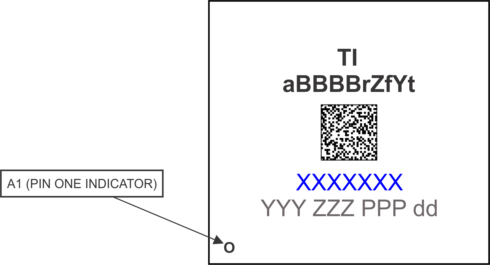
AM625SIP Printed Device
          Reference Figure 8-1 Printed Device Reference