SPRSP89A December   2023  – December 2024 AM62P , AM62P-Q1

ADVANCE INFORMATION  

  1.   1
  2. Features
  3. Applications
  4. Description
    1. 3.1 Functional Block Diagram
  5. Device Comparison
    1. 4.1 Related Products
  6. Terminal Configuration and Functions
    1. 5.1 Pin Diagrams
    2. 5.2 Pin Attributes
      1.      11
      2.      12
    3. 5.3 Signal Descriptions
      1.      14
      2. 5.3.1  CPSW3G
        1. 5.3.1.1 MAIN Domain
          1.        17
          2.        18
          3.        19
          4.        20
      3. 5.3.2  CPTS
        1. 5.3.2.1 MAIN Domain
          1.        23
      4. 5.3.3  CSI-2
        1. 5.3.3.1 MAIN Domain
          1.        26
      5. 5.3.4  DDRSS
        1. 5.3.4.1 MAIN Domain
          1.        29
      6. 5.3.5  DSI
        1. 5.3.5.1 MAIN Domain
          1.        32
      7. 5.3.6  DSS
        1. 5.3.6.1 MAIN Domain
          1.        35
      8. 5.3.7  ECAP
        1. 5.3.7.1 MAIN Domain
          1.        38
          2.        39
          3.        40
      9. 5.3.8  Emulation and Debug
        1. 5.3.8.1 MAIN Domain
          1.        43
        2. 5.3.8.2 MCU Domain
          1.        45
      10. 5.3.9  EPWM
        1. 5.3.9.1 MAIN Domain
          1.        48
          2.        49
          3.        50
          4.        51
      11. 5.3.10 EQEP
        1. 5.3.10.1 MAIN Domain
          1.        54
          2.        55
          3.        56
      12. 5.3.11 GPIO
        1. 5.3.11.1 MAIN Domain
          1.        59
          2.        60
        2. 5.3.11.2 MCU Domain
          1.        62
      13. 5.3.12 GPMC
        1. 5.3.12.1 MAIN Domain
          1.        65
      14. 5.3.13 I2C
        1. 5.3.13.1 MAIN Domain
          1.        68
          2.        69
          3.        70
          4.        71
        2. 5.3.13.2 MCU Domain
          1.        73
        3. 5.3.13.3 WKUP Domain
          1.        75
      15. 5.3.14 MCAN
        1. 5.3.14.1 MAIN Domain
          1.        78
          2.        79
        2. 5.3.14.2 MCU Domain
          1.        81
          2.        82
      16. 5.3.15 MCASP
        1. 5.3.15.1 MAIN Domain
          1.        85
          2.        86
          3.        87
      17. 5.3.16 MCSPI
        1. 5.3.16.1 MAIN Domain
          1.        90
          2.        91
          3.        92
        2. 5.3.16.2 MCU Domain
          1.        94
          2.        95
      18. 5.3.17 MDIO
        1. 5.3.17.1 MAIN Domain
          1.        98
      19. 5.3.18 MMC
        1. 5.3.18.1 MAIN Domain
          1.        101
          2.        102
          3.        103
      20. 5.3.19 OLDI
        1. 5.3.19.1 MAIN Domain
          1.        106
      21. 5.3.20 OSPI
        1. 5.3.20.1 MAIN Domain
          1.        109
      22. 5.3.21 Power Supply
        1.       111
      23. 5.3.22 Reserved
        1.       113
      24. 5.3.23 System and Miscellaneous
        1. 5.3.23.1 Boot Mode Configuration
          1. 5.3.23.1.1 MAIN Domain
            1.         117
        2. 5.3.23.2 Clock
          1. 5.3.23.2.1 MCU Domain
            1.         120
          2. 5.3.23.2.2 WKUP Domain
            1.         122
        3. 5.3.23.3 System
          1. 5.3.23.3.1 MAIN Domain
            1.         125
          2. 5.3.23.3.2 MCU Domain
            1.         127
          3. 5.3.23.3.3 WKUP Domain
            1.         129
        4. 5.3.23.4 VMON
          1.        131
      25. 5.3.24 TIMER
        1. 5.3.24.1 MAIN Domain
          1.        134
        2. 5.3.24.2 MCU Domain
          1.        136
        3. 5.3.24.3 WKUP Domain
          1.        138
      26. 5.3.25 UART
        1. 5.3.25.1 MAIN Domain
          1.        141
          2.        142
          3.        143
          4.        144
          5.        145
          6.        146
          7.        147
        2. 5.3.25.2 MCU Domain
          1.        149
        3. 5.3.25.3 WKUP Domain
          1.        151
      27. 5.3.26 USB
        1. 5.3.26.1 MAIN Domain
          1.        154
          2.        155
    4. 5.4 Pin Connectivity Requirements
  7. Specifications
    1. 6.1  Absolute Maximum Ratings
    2. 6.2  ESD Ratings for Devices which are not AEC - Q100 Qualified
    3. 6.3  ESD Ratings for AEC - Q100 Qualified Devices
    4. 6.4  Power-On Hours (POH)
    5. 6.5  Recommended Operating Conditions
    6. 6.6  Operating Performance Points
    7. 6.7  Power Consumption Summary
    8. 6.8  Electrical Characteristics
      1. 6.8.1  I2C Open-Drain, and Fail-Safe (I2C OD FS) Electrical Characteristics
      2. 6.8.2  Fail-Safe Reset (FS RESET) Electrical Characteristics
      3. 6.8.3  High-Frequency Oscillator (HFOSC) Electrical Characteristics
      4. 6.8.4  Low-Frequency Oscillator (LFXOSC) Electrical Characteristics
      5. 6.8.5  eMMCPHY Electrical Characteristics
      6. 6.8.6  SDIO Electrical Characteristics
      7. 6.8.7  LVCMOS Electrical Characteristics
      8. 6.8.8  OLDI LVDS (OLDI) Electrical Characteristics
      9. 6.8.9  CSI-2 (D-PHY) Electrical Characteristics
      10. 6.8.10 DSI (D-PHY) Electrical Characteristics
      11. 6.8.11 USB2PHY Electrical Characteristics
      12. 6.8.12 DDR Electrical Characteristics
    9. 6.9  VPP Specifications for One-Time Programmable (OTP) eFuses
      1. 6.9.1 Recommended Operating Conditions for OTP eFuse Programming
      2. 6.9.2 Hardware Requirements
      3. 6.9.3 Programming Sequence
      4. 6.9.4 Impact to Your Hardware Warranty
    10. 6.10 Thermal Resistance Characteristics
      1. 6.10.1 Thermal Resistance Characteristics for AMH Package
    11. 6.11 Temperature Sensor Characteristics
    12. 6.12 Timing and Switching Characteristics
      1. 6.12.1 Timing Parameters and Information
      2. 6.12.2 Power Supply Requirements
        1. 6.12.2.1 Power Supply Slew Rate Requirement
        2. 6.12.2.2 Power Supply Sequencing
          1. 6.12.2.2.1 Power-Up Sequencing
          2. 6.12.2.2.2 Power-Down Sequencing
          3. 6.12.2.2.3 Partial IO Power Sequencing
      3. 6.12.3 System Timing
        1. 6.12.3.1 Reset Timing
        2. 6.12.3.2 Error Signal Timing
        3. 6.12.3.3 Clock Timing
      4. 6.12.4 Clock Specifications
        1. 6.12.4.1 Input Clocks / Oscillators
          1. 6.12.4.1.1 MCU_OSC0 Internal Oscillator Clock Source
            1. 6.12.4.1.1.1 Load Capacitance
            2. 6.12.4.1.1.2 Shunt Capacitance
          2. 6.12.4.1.2 MCU_OSC0 LVCMOS Digital Clock Source
          3. 6.12.4.1.3 WKUP_LFOSC0 Internal Oscillator Clock Source
          4. 6.12.4.1.4 WKUP_LFOSC0 LVCMOS Digital Clock Source
          5. 6.12.4.1.5 WKUP_LFOSC0 Not Used
        2. 6.12.4.2 Output Clocks
        3. 6.12.4.3 PLLs
        4. 6.12.4.4 Recommended System Precautions for Clock and Control Signal Transitions
      5. 6.12.5 Peripherals
        1. 6.12.5.1  CPSW3G
          1. 6.12.5.1.1 CPSW3G MDIO Timing
          2. 6.12.5.1.2 CPSW3G RMII Timing
          3. 6.12.5.1.3 CPSW3G RGMII Timing
        2. 6.12.5.2  CPTS
        3. 6.12.5.3  CSI-2
        4. 6.12.5.4  DDRSS
        5. 6.12.5.5  DSI
        6. 6.12.5.6  DSS
        7. 6.12.5.7  ECAP
        8. 6.12.5.8  Emulation and Debug
          1. 6.12.5.8.1 Trace
          2. 6.12.5.8.2 JTAG
        9. 6.12.5.9  EPWM
        10. 6.12.5.10 EQEP
        11. 6.12.5.11 GPIO
        12. 6.12.5.12 GPMC
          1. 6.12.5.12.1 GPMC and NOR Flash — Synchronous Mode
          2. 6.12.5.12.2 GPMC and NOR Flash — Asynchronous Mode
          3. 6.12.5.12.3 GPMC and NAND Flash — Asynchronous Mode
        13. 6.12.5.13 I2C
        14. 6.12.5.14 MCAN
        15. 6.12.5.15 MCASP
        16. 6.12.5.16 MCSPI
          1. 6.12.5.16.1 MCSPI — Controller Mode
          2. 6.12.5.16.2 MCSPI — Peripheral Mode
        17. 6.12.5.17 MMCSD
          1. 6.12.5.17.1 MMC0 - eMMC Interface
            1. 6.12.5.17.1.1 Legacy SDR Mode
            2. 6.12.5.17.1.2 High Speed SDR Mode
            3. 6.12.5.17.1.3 High Speed DDR Mode
            4. 6.12.5.17.1.4 HS200 Mode
            5. 6.12.5.17.1.5 HS400 Mode
          2. 6.12.5.17.2 MMC1/MMC2 - SD/SDIO Interface
            1. 6.12.5.17.2.1 Default Speed Mode
            2. 6.12.5.17.2.2 High Speed Mode
            3. 6.12.5.17.2.3 UHS–I SDR12 Mode
            4. 6.12.5.17.2.4 UHS–I SDR25 Mode
            5. 6.12.5.17.2.5 UHS–I SDR50 Mode
            6. 6.12.5.17.2.6 UHS–I DDR50 Mode
            7. 6.12.5.17.2.7 UHS–I SDR104 Mode
        18. 6.12.5.18 OLDI
          1. 6.12.5.18.1 OLDI0 Switching Characteristics
        19. 6.12.5.19 OSPI
          1. 6.12.5.19.1 OSPI0 PHY Mode
            1. 6.12.5.19.1.1 OSPI0 With PHY Data Training
            2. 6.12.5.19.1.2 OSPI0 Without Data Training
              1. 6.12.5.19.1.2.1 OSPI0 PHY SDR Timing
              2. 6.12.5.19.1.2.2 OSPI0 PHY DDR Timing
          2. 6.12.5.19.2 OSPI0 Tap Mode
            1. 6.12.5.19.2.1 OSPI0 Tap SDR Timing
            2. 6.12.5.19.2.2 OSPI0 Tap DDR Timing
        20. 6.12.5.20 Timers
        21. 6.12.5.21 UART
        22. 6.12.5.22 USB
  8. Detailed Description
    1. 7.1 Overview
    2. 7.2 Processor Subsystems
      1. 7.2.1 Arm Cortex-A53 Subsystem
      2. 7.2.2 Device/Power Manager
      3. 7.2.3 MCU Arm Cortex-R5F Subsystem
    3. 7.3 Accelerators and Coprocessors
      1. 7.3.1 Graphics Processing Unit (GPU)
      2. 7.3.2 Video Accelerator
    4. 7.4 Other Subsystems
      1. 7.4.1 Dual Clock Comparator (DCC)
      2. 7.4.2 Data Movement Subsystem (DMSS)
      3. 7.4.3 Memory Cyclic Redundancy Check (MCRC)
      4. 7.4.4 Peripheral DMA Controller (PDMA)
      5. 7.4.5 Real-Time Clock (RTC)
    5. 7.5 Peripherals
      1. 7.5.1  Gigabit Ethernet Switch (CPSW3G)
      2. 7.5.2  Camera Serial Interface Receiver (CSI_RX_IF)
      3. 7.5.3  Display Subsystem (DSS)
      4. 7.5.4  Enhanced Capture (ECAP)
      5. 7.5.5  Error Location Module (ELM)
      6. 7.5.6  Enhanced Pulse Width Modulation (EPWM)
      7. 7.5.7  Error Signaling Module (ESM)
      8. 7.5.8  Enhanced Quadrature Encoder Pulse (EQEP)
      9. 7.5.9  General-Purpose Interface (GPIO)
      10. 7.5.10 General-Purpose Memory Controller (GPMC)
      11. 7.5.11 Global Timebase Counter (GTC)
      12. 7.5.12 Inter-Integrated Circuit (I2C)
      13. 7.5.13 Modular Controller Area Network (MCAN)
      14. 7.5.14 Multichannel Audio Serial Port (MCASP)
      15. 7.5.15 Multichannel Serial Peripheral Interface (MCSPI)
      16. 7.5.16 Multi-Media Card Secure Digital (MMCSD)
      17. 7.5.17 Octal Serial Peripheral Interface (OSPI)
      18. 7.5.18 Timers
      19. 7.5.19 Universal Asynchronous Receiver/Transmitter (UART)
      20. 7.5.20 Universal Serial Bus Subsystem (USBSS)
  9. Applications, Implementation, and Layout
    1. 8.1 Device Connection and Layout Fundamentals
      1. 8.1.1 Power Supply
        1. 8.1.1.1 Power Supply Designs
        2. 8.1.1.2 Power Distribution Network Implementation Guidance
      2. 8.1.2 External Oscillator
      3. 8.1.3 JTAG, EMU, and TRACE
      4. 8.1.4 Unused Pins
    2. 8.2 Peripheral- and Interface-Specific Design Information
      1. 8.2.1 DDR Board Design and Layout Guidelines
      2. 8.2.2 OSPI/QSPI/SPI Board Design and Layout Guidelines
        1. 8.2.2.1 No Loopback, Internal PHY Loopback, and Internal Pad Loopback
        2. 8.2.2.2 External Board Loopback
        3. 8.2.2.3 DQS (only available in Octal SPI devices)
      3. 8.2.3 USB VBUS Design Guidelines
      4. 8.2.4 System Power Supply Monitor Design Guidelines
      5. 8.2.5 High Speed Differential Signal Routing Guidance
      6. 8.2.6 Thermal Solution Guidance
    3. 8.3 Clock Routing Guidelines
      1. 8.3.1 Oscillator Routing
  10. Device and Documentation Support
    1. 9.1 Device Nomenclature
      1. 9.1.1 Standard Package Symbolization
      2. 9.1.2 Device Naming Convention
    2. 9.2 Tools and Software
    3. 9.3 Documentation Support
    4. 9.4 Support Resources
    5. 9.5 Trademarks
    6. 9.6 Electrostatic Discharge Caution
    7. 9.7 Glossary
  11. 10Revision History
  12. 11Mechanical, Packaging, and Orderable Information
    1. 11.1 Packaging Information

Package Options

Refer to the PDF data sheet for device specific package drawings

Mechanical Data (Package|Pins)
  • AMH|466
Thermal pad, mechanical data (Package|Pins)
Orderable Information
MCSPI — Controller Mode

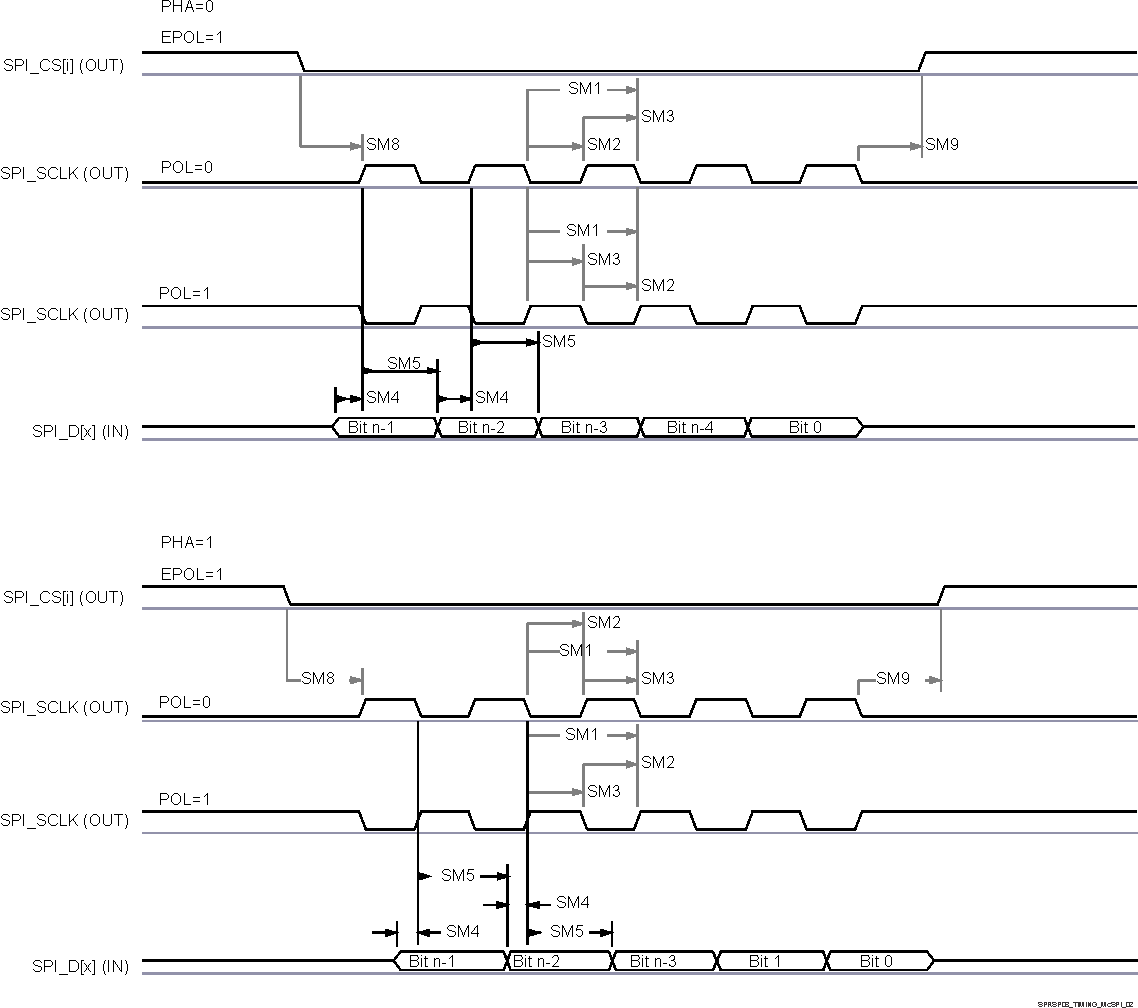
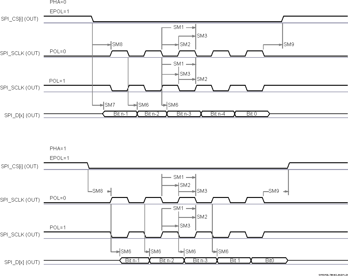
Table 6-77, Figure 6-32, Table 6-78, and Figure 6-64 present timing requirements and switching characteristics for SPI – Controller Mode.

Table 6-77 MCSPI Timing Requirements – Controller Mode see Figure 6-63
NO. PARAMETER DESCRIPTION MIN MAX UNIT
SM4 tsu(POCI-SPICLK) Setup time, SPIn_D[x] valid before SPIn_CLK active edge 2.8 ns
SM5 th(SPICLK-POCI) Hold time, SPIn_D[x] valid after SPIn_CLK active edge 3 ns
AM62P AM62P-Q1 SPI Controller Mode Receive
                    Timing Figure 6-63 SPI Controller Mode Receive Timing
Table 6-78 MCSPI Switching Characteristics - Controller Mode see Figure 6-64
NO. PARAMETER MIN MAX UNIT
SM1 tc(SPICLK) Cycle time, SPIn_CLK 20 ns
SM2 tw(SPICLKL) Pulse duration, SPIn_CLK low 0.5P - 1(1) ns
SM3 tw(SPICLKH) Pulse duration, SPIn_CLK high 0.5P - 1(1) ns
SM6 td(SPICLK-PICO) Delay time, SPIn_CLK active edge to SPIn_D[x] -3 2.5 ns
SM7 td(CS-PICO) Delay time, SPIn_CSi active edge to SPIn_D[x] 5 ns
SM8 td(CS-SPICLK) Delay time, SPIn_CSi active to SPIn_CLK first edge PHA = 0 B - 4 (2) ns
PHA = 1 A - 4 (3) ns
SM9 td(SPICLK-CS) Delay time, SPIn_CLK last edge to SPIn_CSi inactive PHA = 0 A - 4(4) ns
PHA = 1 B - 4(5) ns
P = SPIn_CLK period in ns.
T_ref is the period of the McSPI functional clock in ns. Fratio is the divide ratio of McSPI functional clock frequency to SPIn_CLK clock frequency, controlled by the CLKD and CLKG bit fields in the MSPI_CH(i)CONF register and the EXTCLK bit field in the MSPI_CH(i)CTRL register. TCS(i) is the value programmed into the chip select time control bit field of the MSPI_CH(i)CONF register.
  • When Fratio = 1; B = (TCS(i) + 0.5) * T_ref.
  • When Fratio ≥ 2 and even value; B = (TCS(i) + 0.5) * Fratio * T_ref.
  • When Fratio ≥ 3 and odd value; B = ((TCS(i) * Fratio) + ((Fratio + 1) / 2 )) * T_ref.
T_ref is the period of the McSPI functional clock. Fratio is the divide ratio of McSPI functional clock frequency to SPIn_CLK clock frequency, controlled by the CLKD and CLKG bit fields in the MSPI_CH(i)CONF register and the EXTCLK bit field in the MSPI_CH(i)CTRL register. TCS(i) is the value programmed into the chip select time control bit field of the MSPI_CH(i)CONF register.
  • When Fratio = 1; A = (TCS(i) + 1) * T_ref.
  • When Fratio ≥ 2 and even value; A = (TCS(i) + 0.5) * Fratio * T_ref.
  • When Fratio ≥ 3 and odd value; A = ((TCS(i) * Fratio) + ((Fratio - 1) / 2 )) * T_ref.
T_ref is the period of the McSPI functional clock. Fratio is the divide ratio of McSPI functional clock frequency to SPIn_CLK clock frequency, controlled by the CLKD and CLKG bit fields in the MSPI_CH(i)CONF register and the EXTCLK bit field in the MSPI_CH(i)CTRL register. TCS(i) is the value programmed into the chip select time control bit field of the MSPI_CH(i)CONF register.
  • When Fratio = 1; A = (TCS(i) + 1) * T_ref.
  • When Fratio ≥ 2 and even value; A = (TCS(i) + 0.5) * Fratio * T_ref.
  • When Fratio ≥ 3 and odd value; A = ((TCS(i) * Fratio) + ((Fratio + 1) / 2 )) * T_ref.
T_ref is the period of the McSPI functional clock. Fratio is the divide ratio of McSPI functional clock frequency to SPIn_CLK clock frequency, controlled by the CLKD and CLKG bit fields in the MSPI_CH(i)CONF register and the EXTCLK bit field in the MSPI_CH(i)CTRL register. TCS(i) is the value programmed into the chip select time control bit field of the MSPI_CH(i)CONF register.
  • When Fratio = 1; B = (TCS(i) + 0.5) * T_ref.
  • When Fratio ≥ 2 and even value; B = (TCS(i) + 0.5) * Fratio * T_ref.
  • When Fratio ≥ 3 and odd value; B = ((TCS(i) * Fratio) + ((Fratio - 1) / 2 )) * T_ref.
AM62P AM62P-Q1 SPI Controller Mode Transmit
                    Timing Figure 6-64 SPI Controller Mode Transmit Timing