SPRSP89A December 2023 – December 2024 AM62P , AM62P-Q1
ADVANCE INFORMATION
- 1
- 1 Features
- 2 Applications
- 3 Description
- 4 Device Comparison
-
5 Terminal Configuration and Functions
- 5.1 Pin Diagrams
- 5.2 Pin Attributes
- 5.3
Signal Descriptions
- 14
- 5.3.1 CPSW3G
- 5.3.2 CPTS
- 5.3.3 CSI-2
- 5.3.4 DDRSS
- 5.3.5 DSI
- 5.3.6 DSS
- 5.3.7 ECAP
- 5.3.8 Emulation and Debug
- 5.3.9 EPWM
- 5.3.10 EQEP
- 5.3.11 GPIO
- 5.3.12 GPMC
- 5.3.13 I2C
- 5.3.14 MCAN
- 5.3.15 MCASP
- 5.3.16 MCSPI
- 5.3.17 MDIO
- 5.3.18 MMC
- 5.3.19 OLDI
- 5.3.20 OSPI
- 5.3.21 Power Supply
- 5.3.22 Reserved
- 5.3.23 System and Miscellaneous
- 5.3.24 TIMER
- 5.3.25 UART
- 5.3.26 USB
- 5.4 Pin Connectivity Requirements
-
6 Specifications
- 6.1 Absolute Maximum Ratings
- 6.2 ESD Ratings for Devices which are not AEC - Q100 Qualified
- 6.3 ESD Ratings for AEC - Q100 Qualified Devices
- 6.4 Power-On Hours (POH)
- 6.5 Recommended Operating Conditions
- 6.6 Operating Performance Points
- 6.7 Power Consumption Summary
- 6.8
Electrical
Characteristics
- 6.8.1 I2C Open-Drain, and Fail-Safe (I2C OD FS) Electrical Characteristics
- 6.8.2 Fail-Safe Reset (FS RESET) Electrical Characteristics
- 6.8.3 High-Frequency Oscillator (HFOSC) Electrical Characteristics
- 6.8.4 Low-Frequency Oscillator (LFXOSC) Electrical Characteristics
- 6.8.5 eMMCPHY Electrical Characteristics
- 6.8.6 SDIO Electrical Characteristics
- 6.8.7 LVCMOS Electrical Characteristics
- 6.8.8 OLDI LVDS (OLDI) Electrical Characteristics
- 6.8.9 CSI-2 (D-PHY) Electrical Characteristics
- 6.8.10 DSI (D-PHY) Electrical Characteristics
- 6.8.11 USB2PHY Electrical Characteristics
- 6.8.12 DDR Electrical Characteristics
- 6.9 VPP Specifications for One-Time Programmable (OTP) eFuses
- 6.10 Thermal Resistance Characteristics
- 6.11 Temperature Sensor Characteristics
- 6.12
Timing and Switching Characteristics
- 6.12.1 Timing Parameters and Information
- 6.12.2 Power Supply Requirements
- 6.12.3 System Timing
- 6.12.4
Clock Specifications
- 6.12.4.1 Input Clocks / Oscillators
- 6.12.4.2 Output Clocks
- 6.12.4.3 PLLs
- 6.12.4.4 Recommended System Precautions for Clock and Control Signal Transitions
- 6.12.5
Peripherals
- 6.12.5.1 CPSW3G
- 6.12.5.2 CPTS
- 6.12.5.3 CSI-2
- 6.12.5.4 DDRSS
- 6.12.5.5 DSI
- 6.12.5.6 DSS
- 6.12.5.7 ECAP
- 6.12.5.8 Emulation and Debug
- 6.12.5.9 EPWM
- 6.12.5.10 EQEP
- 6.12.5.11 GPIO
- 6.12.5.12 GPMC
- 6.12.5.13 I2C
- 6.12.5.14 MCAN
- 6.12.5.15 MCASP
- 6.12.5.16 MCSPI
- 6.12.5.17 MMCSD
- 6.12.5.18 OLDI
- 6.12.5.19 OSPI
- 6.12.5.20 Timers
- 6.12.5.21 UART
- 6.12.5.22 USB
-
7 Detailed Description
- 7.1 Overview
- 7.2 Processor Subsystems
- 7.3 Accelerators and Coprocessors
- 7.4 Other Subsystems
- 7.5
Peripherals
- 7.5.1 Gigabit Ethernet Switch (CPSW3G)
- 7.5.2 Camera Serial Interface Receiver (CSI_RX_IF)
- 7.5.3 Display Subsystem (DSS)
- 7.5.4 Enhanced Capture (ECAP)
- 7.5.5 Error Location Module (ELM)
- 7.5.6 Enhanced Pulse Width Modulation (EPWM)
- 7.5.7 Error Signaling Module (ESM)
- 7.5.8 Enhanced Quadrature Encoder Pulse (EQEP)
- 7.5.9 General-Purpose Interface (GPIO)
- 7.5.10 General-Purpose Memory Controller (GPMC)
- 7.5.11 Global Timebase Counter (GTC)
- 7.5.12 Inter-Integrated Circuit (I2C)
- 7.5.13 Modular Controller Area Network (MCAN)
- 7.5.14 Multichannel Audio Serial Port (MCASP)
- 7.5.15 Multichannel Serial Peripheral Interface (MCSPI)
- 7.5.16 Multi-Media Card Secure Digital (MMCSD)
- 7.5.17 Octal Serial Peripheral Interface (OSPI)
- 7.5.18 Timers
- 7.5.19 Universal Asynchronous Receiver/Transmitter (UART)
- 7.5.20 Universal Serial Bus Subsystem (USBSS)
-
8 Applications,
Implementation, and Layout
- 8.1 Device Connection and Layout Fundamentals
- 8.2 Peripheral- and Interface-Specific Design Information
- 8.3 Clock Routing Guidelines
- 9 Device and Documentation Support
- 10Revision History
- 11Mechanical, Packaging, and Orderable Information
Package Options
Refer to the PDF data sheet for device specific package drawings
Mechanical Data (Package|Pins)
- AMH|466
Thermal pad, mechanical data (Package|Pins)
Orderable Information
6.12.4.1.1.1 Load Capacitance
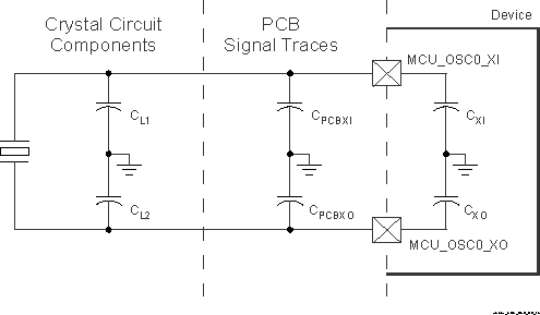
The crystal circuit must be designed such that it applies the appropriate capacitive load to the crystal, as defined by the crystal manufacturer. The capacitive load, CL, of this circuit is a combination of discrete capacitors CL1, CL2, and several parasitic contributions. PCB signal traces which connect crystal circuit components to MCU_OSC0_XI and MCU_OSC0_XO have parasitic capacitance to ground, CPCBXI and CPCBXO, where the PCB designer should be able to extract parasitic capacitance for each signal trace. The MCU_OSC0 circuits and device package have combined parasitic capacitance to ground, CPCBXI and CPCBXO, where these parasitic capacitance values are defined in Table 6-23.
 Figure 6-18 Load Capacitance
Load capacitors, CL1 and CL2 in Figure 6-16, should be chosen such that the below equation is satisfied. CL in the equation is the load specified by the crystal manufacturer.
CL = [(CL1 + CPCBXI + CXI) × (CL2 + CPCBXO + CXO)] / [(CL1 + CPCBXI + CXI) + (CL2 + CPCBXO + CXO)]
To determine the value of CL1 and CL2, multiply the capacitive load value CL by 2. Using this result, subtract the combined values of CPCBXI + CXI to determine the value of CL1 and the combined values of CPCBXO + CXO to determine the value of CL2. For example, if CL = 10pF, CPCBXI = 2.9pF, CXI = 0.5pF, CPCBXO = 3.7pF, CXO = 0.5pF, the value of CL1 = [(2CL) - (CPCBXI + CXI)] = [(2 × 10pF) - 2.9pF - 0.5pF)] = 16.6pF and CL2 = [(2CL) - (CPCBXO + CXO)] = [(2 × 10pF) - 3.7pF - 0.5pF)] = 15.8pF