SPRSP89A December 2023 – December 2024 AM62P , AM62P-Q1
ADVANCE INFORMATION
- 1
- 1 Features
- 2 Applications
- 3 Description
- 4 Device Comparison
-
5 Terminal Configuration and Functions
- 5.1 Pin Diagrams
- 5.2 Pin Attributes
- 5.3
Signal Descriptions
- 14
- 5.3.1 CPSW3G
- 5.3.2 CPTS
- 5.3.3 CSI-2
- 5.3.4 DDRSS
- 5.3.5 DSI
- 5.3.6 DSS
- 5.3.7 ECAP
- 5.3.8 Emulation and Debug
- 5.3.9 EPWM
- 5.3.10 EQEP
- 5.3.11 GPIO
- 5.3.12 GPMC
- 5.3.13 I2C
- 5.3.14 MCAN
- 5.3.15 MCASP
- 5.3.16 MCSPI
- 5.3.17 MDIO
- 5.3.18 MMC
- 5.3.19 OLDI
- 5.3.20 OSPI
- 5.3.21 Power Supply
- 5.3.22 Reserved
- 5.3.23 System and Miscellaneous
- 5.3.24 TIMER
- 5.3.25 UART
- 5.3.26 USB
- 5.4 Pin Connectivity Requirements
-
6 Specifications
- 6.1 Absolute Maximum Ratings
- 6.2 ESD Ratings for Devices which are not AEC - Q100 Qualified
- 6.3 ESD Ratings for AEC - Q100 Qualified Devices
- 6.4 Power-On Hours (POH)
- 6.5 Recommended Operating Conditions
- 6.6 Operating Performance Points
- 6.7 Power Consumption Summary
- 6.8
Electrical
Characteristics
- 6.8.1 I2C Open-Drain, and Fail-Safe (I2C OD FS) Electrical Characteristics
- 6.8.2 Fail-Safe Reset (FS RESET) Electrical Characteristics
- 6.8.3 High-Frequency Oscillator (HFOSC) Electrical Characteristics
- 6.8.4 Low-Frequency Oscillator (LFXOSC) Electrical Characteristics
- 6.8.5 eMMCPHY Electrical Characteristics
- 6.8.6 SDIO Electrical Characteristics
- 6.8.7 LVCMOS Electrical Characteristics
- 6.8.8 OLDI LVDS (OLDI) Electrical Characteristics
- 6.8.9 CSI-2 (D-PHY) Electrical Characteristics
- 6.8.10 DSI (D-PHY) Electrical Characteristics
- 6.8.11 USB2PHY Electrical Characteristics
- 6.8.12 DDR Electrical Characteristics
- 6.9 VPP Specifications for One-Time Programmable (OTP) eFuses
- 6.10 Thermal Resistance Characteristics
- 6.11 Temperature Sensor Characteristics
- 6.12
Timing and Switching Characteristics
- 6.12.1 Timing Parameters and Information
- 6.12.2 Power Supply Requirements
- 6.12.3 System Timing
- 6.12.4
Clock Specifications
- 6.12.4.1 Input Clocks / Oscillators
- 6.12.4.2 Output Clocks
- 6.12.4.3 PLLs
- 6.12.4.4 Recommended System Precautions for Clock and Control Signal Transitions
- 6.12.5
Peripherals
- 6.12.5.1 CPSW3G
- 6.12.5.2 CPTS
- 6.12.5.3 CSI-2
- 6.12.5.4 DDRSS
- 6.12.5.5 DSI
- 6.12.5.6 DSS
- 6.12.5.7 ECAP
- 6.12.5.8 Emulation and Debug
- 6.12.5.9 EPWM
- 6.12.5.10 EQEP
- 6.12.5.11 GPIO
- 6.12.5.12 GPMC
- 6.12.5.13 I2C
- 6.12.5.14 MCAN
- 6.12.5.15 MCASP
- 6.12.5.16 MCSPI
- 6.12.5.17 MMCSD
- 6.12.5.18 OLDI
- 6.12.5.19 OSPI
- 6.12.5.20 Timers
- 6.12.5.21 UART
- 6.12.5.22 USB
-
7 Detailed Description
- 7.1 Overview
- 7.2 Processor Subsystems
- 7.3 Accelerators and Coprocessors
- 7.4 Other Subsystems
- 7.5
Peripherals
- 7.5.1 Gigabit Ethernet Switch (CPSW3G)
- 7.5.2 Camera Serial Interface Receiver (CSI_RX_IF)
- 7.5.3 Display Subsystem (DSS)
- 7.5.4 Enhanced Capture (ECAP)
- 7.5.5 Error Location Module (ELM)
- 7.5.6 Enhanced Pulse Width Modulation (EPWM)
- 7.5.7 Error Signaling Module (ESM)
- 7.5.8 Enhanced Quadrature Encoder Pulse (EQEP)
- 7.5.9 General-Purpose Interface (GPIO)
- 7.5.10 General-Purpose Memory Controller (GPMC)
- 7.5.11 Global Timebase Counter (GTC)
- 7.5.12 Inter-Integrated Circuit (I2C)
- 7.5.13 Modular Controller Area Network (MCAN)
- 7.5.14 Multichannel Audio Serial Port (MCASP)
- 7.5.15 Multichannel Serial Peripheral Interface (MCSPI)
- 7.5.16 Multi-Media Card Secure Digital (MMCSD)
- 7.5.17 Octal Serial Peripheral Interface (OSPI)
- 7.5.18 Timers
- 7.5.19 Universal Asynchronous Receiver/Transmitter (UART)
- 7.5.20 Universal Serial Bus Subsystem (USBSS)
-
8 Applications,
Implementation, and Layout
- 8.1 Device Connection and Layout Fundamentals
- 8.2 Peripheral- and Interface-Specific Design Information
- 8.3 Clock Routing Guidelines
- 9 Device and Documentation Support
- 10Revision History
- 11Mechanical, Packaging, and Orderable Information
Package Options
Refer to the PDF data sheet for device specific package drawings
Mechanical Data (Package|Pins)
- AMH|466
Thermal pad, mechanical data (Package|Pins)
Orderable Information
8.2.2.2 External Board Loopback
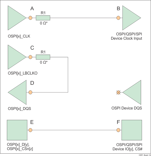
- The OSPI[x]_CLK output pin must be connected to the CLK input pin of the attached OSPI/QSPI/SPI device
- The OSPI[x]_LBCLKO output pin must be looped back to the OSPI[x]_DQS input pin
- The signal propagation delay of the OSPI[x]_LBCLKO pin to the OSPI[x]_DQS pin (C to D) must be approximately twice the propagation delay of the OSPI[x]_CLK pin to the attached OSPI/QSPI/SPI device CLK pin (A to B)
- The signal propagation delay of each OSPI[x]_D[y] and OSPI[x]_CSn[z] pin to the corresponding attached OSPI/QSPI/SPI device data and control pin (E to F, or F to E) must be approximately equal to the signal propagation delay from the OSPI[x]_CLK pin to the attached OSPI/QSPI/SPI device CLK pin (A to B)
- 50Ω PCB routing is recommended along with series terminations, as shown in Figure 8-2
- Propagation delays and matching:
- (C to D) = 2 x ((A to B) ± 30ps), see the exception note below.
- (E to F, or F to E) = ((A to B) ± 60ps)
Note:
The External Board Loopback hold time requirement (defined by parameter number O16 in the OSPI0 Timing Requirements - PHY DDR Mode section) may be larger than the hold time provided by a typical OSPI/QSPI/SPI device. In this case, the propagation delay of OPSI[x]_LBCLKO pin to the OSPI[x]_DQS pin (C to D) can be reduced to provide additional hold time.

* 0Ω resistor
(R1), located as close as possible to the OSPI[x]_CLK and OSPI[x]_LBCLKO pins,
is a placeholder for fine tuning, if needed.
Figure 8-2 OSPI
Connectivity Schematic for External Board Loopback