SPRSPA3A March   2024  – September 2024 AM67 , AM67A

PRODUCTION DATA  

  1.   1
  2. Features
  3. Applications
  4. Description
    1. 3.1 Functional Block Diagram
  5. Device Comparison
  6. Terminal Configuration and Functions
    1. 5.1 Pin Diagrams
    2. 5.2 Pin Attributes
      1.      10
      2.      11
    3. 5.3 Signal Descriptions
      1.      13
      2. 5.3.1  CPSW3G
        1. 5.3.1.1 MAIN Domain
          1.        16
          2.        17
          3.        18
          4.        19
      3. 5.3.2  CPTS
        1. 5.3.2.1 MAIN Domain
          1.        22
      4. 5.3.3  CSI-2
        1. 5.3.3.1 MAIN Domain
          1.        25
          2.        26
          3.        27
          4.        28
      5. 5.3.4  DDRSS
        1. 5.3.4.1 MAIN Domain
          1.        31
      6. 5.3.5  DSI
        1. 5.3.5.1 MAIN Domain
          1.        34
      7. 5.3.6  DSS
        1. 5.3.6.1 MAIN Domain
          1.        37
      8. 5.3.7  ECAP
        1. 5.3.7.1 MAIN Domain
          1.        40
          2.        41
          3.        42
      9. 5.3.8  Emulation and Debug
        1. 5.3.8.1 MAIN Domain
          1.        45
        2. 5.3.8.2 MCU Domain
          1.        47
      10. 5.3.9  EPWM
        1. 5.3.9.1 MAIN Domain
          1.        50
          2.        51
          3.        52
          4.        53
      11. 5.3.10 EQEP
        1. 5.3.10.1 MAIN Domain
          1.        56
          2.        57
          3.        58
      12. 5.3.11 GPIO
        1. 5.3.11.1 MAIN Domain
          1.        61
          2.        62
        2. 5.3.11.2 MCU Domain
          1.        64
      13. 5.3.12 GPMC
        1. 5.3.12.1 MAIN Domain
          1.        67
      14. 5.3.13 I2C
        1. 5.3.13.1 MAIN Domain
          1.        70
          2.        71
          3.        72
          4.        73
          5.        74
        2. 5.3.13.2 MCU Domain
          1.        76
        3. 5.3.13.3 WKUP Domain
          1.        78
      15. 5.3.14 MCAN
        1. 5.3.14.1 MAIN Domain
          1.        81
          2.        82
        2. 5.3.14.2 MCU Domain
          1.        84
          2.        85
      16. 5.3.15 MCASP
        1. 5.3.15.1 MAIN Domain
          1.        88
          2.        89
          3.        90
          4.        91
          5.        92
      17. 5.3.16 MCSPI
        1. 5.3.16.1 MAIN Domain
          1.        95
          2.        96
          3.        97
        2. 5.3.16.2 MCU Domain
          1.        99
          2.        100
      18. 5.3.17 MDIO
        1. 5.3.17.1 MAIN Domain
          1.        103
      19. 5.3.18 MMC
        1. 5.3.18.1 MAIN Domain
          1.        106
          2.        107
          3.        108
      20. 5.3.19 OLDI
        1. 5.3.19.1 MAIN Domain
          1.        111
      21. 5.3.20 OSPI
        1. 5.3.20.1 MAIN Domain
          1.        114
      22. 5.3.21 Power Supply
        1.       116
      23. 5.3.22 Reserved
        1.       118
      24. 5.3.23 SERDES
        1. 5.3.23.1 MAIN Domain
          1.        121
          2.        122
          3.        123
      25. 5.3.24 System and Miscellaneous
        1. 5.3.24.1 Boot Mode Configuration
          1. 5.3.24.1.1 MAIN Domain
            1.         127
        2. 5.3.24.2 Clock
          1. 5.3.24.2.1 MCU Domain
            1.         130
          2. 5.3.24.2.2 WKUP Domain
            1.         132
        3. 5.3.24.3 System
          1. 5.3.24.3.1 MAIN Domain
            1.         135
          2. 5.3.24.3.2 MCU Domain
            1.         137
          3. 5.3.24.3.3 WKUP Domain
            1.         139
        4. 5.3.24.4 VMON
          1.        141
      26. 5.3.25 TIMER
        1. 5.3.25.1 MAIN Domain
          1.        144
        2. 5.3.25.2 MCU Domain
          1.        146
        3. 5.3.25.3 WKUP Domain
          1.        148
      27. 5.3.26 UART
        1. 5.3.26.1 MAIN Domain
          1.        151
          2.        152
          3.        153
          4.        154
          5.        155
          6.        156
          7.        157
        2. 5.3.26.2 MCU Domain
          1.        159
        3. 5.3.26.3 WKUP Domain
          1.        161
      28. 5.3.27 USB
        1. 5.3.27.1 MAIN Domain
          1.        164
          2.        165
    4. 5.4 Pin Connectivity Requirements
  7. Specifications
    1. 6.1 Absolute Maximum Ratings
    2. 6.2 ESD Ratings for Devices which are not AEC - Q100 Qualified
    3. 6.3 Power-On Hours (POH)
    4. 6.4 Recommended Operating Conditions
    5. 6.5 Operating Performance Points
    6. 6.6 Electrical Characteristics
      1. 6.6.1 I2C Open-Drain, and Fail-Safe (I2C OD FS) Electrical Characteristics
      2. 6.6.2 Fail-Safe Reset (FS RESET) Electrical Characteristics
      3. 6.6.3 High-Frequency Oscillator (HFOSC) Electrical Characteristics
      4. 6.6.4 Low-Frequency Oscillator (LFXOSC) Electrical Characteristics
      5. 6.6.5 SDIO Electrical Characteristics
      6. 6.6.6 LVCMOS Electrical Characteristics
      7. 6.6.7 CSI-2 (D-PHY) Electrical Characteristics
      8. 6.6.8 USB2PHY Electrical Characteristics
      9. 6.6.9 DDR Electrical Characteristics
    7. 6.7 VPP Specifications for One-Time Programmable (OTP) eFuses
      1. 6.7.1 Recommended Operating Conditions for OTP eFuse Programming
      2. 6.7.2 Hardware Requirements
      3. 6.7.3 Programming Sequence
      4. 6.7.4 Impact to Your Hardware Warranty
    8. 6.8 Thermal Resistance Characteristics
      1. 6.8.1 Thermal Resistance Characteristics for AMW Package TBD
    9. 6.9 Timing and Switching Characteristics
      1. 6.9.1 Timing Parameters and Information
      2. 6.9.2 Power Supply Requirements
        1. 6.9.2.1 Power Supply Slew Rate Requirement
        2. 6.9.2.2 Power Supply Sequencing
          1. 6.9.2.2.1 Power-Up Sequencing
          2. 6.9.2.2.2 Power-Down Sequencing
          3. 6.9.2.2.3 Partial IO Power Sequencing
      3. 6.9.3 System Timing
        1. 6.9.3.1 Reset Timing
        2. 6.9.3.2 Error Signal Timing
        3. 6.9.3.3 Clock Timing
      4. 6.9.4 Clock Specifications
        1. 6.9.4.1 Input Clocks / Oscillators
          1. 6.9.4.1.1 MCU_OSC0 Internal Oscillator Clock Source
            1. 6.9.4.1.1.1 Load Capacitance
            2. 6.9.4.1.1.2 Shunt Capacitance
          2. 6.9.4.1.2 MCU_OSC0 LVCMOS Digital Clock Source
          3. 6.9.4.1.3 WKUP_LFOSC0 Internal Oscillator Clock Source
          4. 6.9.4.1.4 WKUP_LFOSC0 LVCMOS Digital Clock Source
          5. 6.9.4.1.5 WKUP_LFOSC0 Not Used
        2. 6.9.4.2 Output Clocks
        3. 6.9.4.3 PLLs
        4. 6.9.4.4 Recommended System Precautions for Clock and Control Signal Transitions
      5. 6.9.5 Peripherals
        1. 6.9.5.1  ATL
          1. 6.9.5.1.1 ATL_PCLK Timing Requirements
          2. 6.9.5.1.2 ATL_AWS[x] Timing Requirements
          3. 6.9.5.1.3 ATL_BWS[x] Timing Requirements
          4. 6.9.5.1.4 ATCLK[x] Switching Characteristics
        2. 6.9.5.2  CPSW3G
          1. 6.9.5.2.1 CPSW3G MDIO Timing
          2. 6.9.5.2.2 CPSW3G RMII Timing
          3. 6.9.5.2.3 CPSW3G RGMII Timing
        3. 6.9.5.3  CPTS
        4. 6.9.5.4  CSI-2
        5. 6.9.5.5  CSI-2 TX
        6. 6.9.5.6  DDRSS
        7. 6.9.5.7  DSS
        8. 6.9.5.8  ECAP
        9. 6.9.5.9  Emulation and Debug
          1. 6.9.5.9.1 Trace
          2. 6.9.5.9.2 JTAG
        10. 6.9.5.10 EPWM
        11. 6.9.5.11 EQEP
        12. 6.9.5.12 GPIO
        13. 6.9.5.13 GPMC
          1. 6.9.5.13.1 GPMC and NOR Flash — Synchronous Mode
          2. 6.9.5.13.2 GPMC and NOR Flash — Asynchronous Mode
          3. 6.9.5.13.3 GPMC and NAND Flash — Asynchronous Mode
        14. 6.9.5.14 I2C
        15. 6.9.5.15 MCAN
        16. 6.9.5.16 MCASP
        17. 6.9.5.17 MCSPI
          1. 6.9.5.17.1 MCSPI — Controller Mode
          2. 6.9.5.17.2 MCSPI — Peripheral Mode
        18. 6.9.5.18 MMCSD
          1. 6.9.5.18.1 MMC0 - eMMC Interface
            1. 6.9.5.18.1.1  Legacy SDR Mode
            2. 6.9.5.18.1.2  High Speed SDR Mode
            3. 6.9.5.18.1.3  High Speed DDR Mode
            4. 6.9.5.18.1.4  HS200 Mode
            5. 6.9.5.18.1.5  HS400 Mode
            6. 6.9.5.18.1.6  UHS–I SDR12 Mode
            7. 6.9.5.18.1.7  UHS–I SDR25 Mode
            8. 6.9.5.18.1.8  UHS–I SDR50 Mode
            9. 6.9.5.18.1.9  UHS–I DDR50 Mode
            10. 6.9.5.18.1.10 UHS–I SDR104 Mode
          2. 6.9.5.18.2 MMC1/MMC2 - SD/SDIO Interface
            1. 6.9.5.18.2.1 Default Speed Mode
            2. 6.9.5.18.2.2 High Speed Mode
            3. 6.9.5.18.2.3 UHS–I SDR12 Mode
            4. 6.9.5.18.2.4 UHS–I SDR25 Mode
            5. 6.9.5.18.2.5 UHS–I SDR50 Mode
            6. 6.9.5.18.2.6 UHS–I DDR50 Mode
            7. 6.9.5.18.2.7 UHS–I SDR104 Mode
        19. 6.9.5.19 OSPI
          1. 6.9.5.19.1 OSPI0 PHY Mode
            1. 6.9.5.19.1.1 OSPI0 With PHY Data Training
            2. 6.9.5.19.1.2 OSPI0 Without Data Training
              1. 6.9.5.19.1.2.1 OSPI0 PHY SDR Timing
              2. 6.9.5.19.1.2.2 OSPI0 PHY DDR Timing
          2. 6.9.5.19.2 OSPI0 Tap Mode
            1. 6.9.5.19.2.1 OSPI0 Tap SDR Timing
            2. 6.9.5.19.2.2 OSPI0 Tap DDR Timing
        20. 6.9.5.20 PCIe
        21. 6.9.5.21 Timers
        22. 6.9.5.22 UART
        23. 6.9.5.23 USB
  8. Detailed Description
    1. 7.1 Overview
  9. Applications, Implementation, and Layout
    1. 8.1 Device Connection and Layout Fundamentals
      1. 8.1.1 Power Supply
        1. 8.1.1.1 Power Distribution Network Implementation Guidance
      2. 8.1.2 External Oscillator
      3. 8.1.3 JTAG, EMU, and TRACE
      4. 8.1.4 Unused Pins
    2. 8.2 Peripheral- and Interface-Specific Design Information
      1. 8.2.1 LPDDR4 Board Design and Layout Guidelines
      2. 8.2.2 OSPI/QSPI/SPI Board Design and Layout Guidelines
        1. 8.2.2.1 No Loopback, Internal PHY Loopback, and Internal Pad Loopback
        2. 8.2.2.2 External Board Loopback
        3. 8.2.2.3 DQS (only available in Octal SPI devices)
      3. 8.2.3 USB VBUS Design Guidelines
      4. 8.2.4 System Power Supply Monitor Design Guidelines
      5. 8.2.5 High Speed Differential Signal Routing Guidance
      6. 8.2.6 Thermal Solution Guidance
    3. 8.3 Clock Routing Guidelines
      1. 8.3.1 Oscillator Routing
  10. Device and Documentation Support
    1. 9.1 Device Nomenclature
      1. 9.1.1 Standard Package Symbolization
      2. 9.1.2 Device Naming Convention
    2. 9.2 Tools and Software
    3. 9.3 Documentation Support
    4. 9.4 Support Resources
    5. 9.5 Trademarks
    6. 9.6 Electrostatic Discharge Caution
    7. 9.7 Glossary
  11. 10Revision History
  12. 11Mechanical, Packaging, and Orderable Information
    1. 11.1 Packaging Information

Package Options

Refer to the PDF data sheet for device specific package drawings

Mechanical Data (Package|Pins)
  • AMW|594
Thermal pad, mechanical data (Package|Pins)
Orderable Information

MCU_OSC0 LVCMOS Digital Clock Source

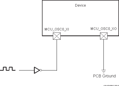
Figure 6-20 shows the recommended oscillator connections when MCU_OSC0_XI is connected to a 1.8V LVCMOS square-wave digital clock source.

Note:
  1. A DC steady-state condition is not allowed on MCU_OSC0_XI when the oscillator is powered up. This is not allowed because MCU_OSC0_XI is internally AC coupled to a comparator that can enter an unknown state when DC is applied to the input. Therefore, application software must power down MCU_OSC0 any time MCU_OSC0_XI is not toggling between logic states.
  2. The LVCMOS clock signal sourcing the MCU_OSC0_XI input must have monotonic transitions. The clock source should be connected to MCU_OSC0_XI with a point-to-point connection, via a series termination resistor placed near the clock source. The series termination resistor value should match the clock source output impedance to the transmission line impedance. For example, the series termination resistor value needs to be 20 ohms if the clock source has an output impedance of 30 ohms and the PCB signal trace has a characteristic impedance of 50 ohms. This allows the reflection that returns from the far end of the un-terminated transmission line to be completely absorbed such that is does not introduce any non-monotonic events on the signal.
  3. The PCB trace length connecting the LVCMOS clock source to MCU_OSC0_XI should be minimized. This reduces capacitive loading and decreases probability of external noise sources coupling into the clock signal. Reduced capacitive loading improves rise/fall times of the clock signal which reduces the probability of jitter being introduced in the system.
AM67 AM67A 1.8V LVCMOS-Compatible
          Clock Input Figure 6-20 1.8V LVCMOS-Compatible Clock Input
Table 6-23 MCU_OSC0 LVCMOS Digital Clock Source Requirements
PARAMETER MIN TYP MAX UNIT
Fxtal Frequency 25 MHz
Frequency Stability and Tolerance Ethernet RGMII and RMII not used ±100 ppm
Ethernet RGMII and RMII using derived clock ±50
DC Duty Cycle 45 55 %
tR/F Rise/Fall Time (10%-90% rise, 90%-10% fall) 4(1) ns
JPeriod(RMS) Period Jitter, RMS (100k samples) 20 ps
JPeriod(PK-PK) Period Jitter, Peak to Peak (100k samples) 300 ps
JPhase(RMS) Phase Jitter, RMS (BW 100Hz to 1MHz) 10(2) ps
Most LVCMOS oscillator datasheets define their maximum Output Rise/Fall times with a capacitive load much larger than the actual load that will be applied by the combined PCB trace capacitance and MCU_OSC0_XI input capacitance. It should not be difficult to find a LVCMOS oscillator that meets this requirement. However, the system designer must confirm the LVCMOS oscillator selected will provide the appropriate rise/fall time to MCU_OSC0_XI input.
Most LVCMOS oscillator datasheets define their max RMS Phase Jitter using a larger bandwidth integration range than required by this device. To get a more appropriate value, it may be necessary to contact the LVCMOS oscillator manufacture and ask them to provide a maximum RMS Phase Jitter using the same bandwidth integration range that has been defined for this parameter.