SPRSP91B February   2023  – December 2024 AM68 , AM68A

PRODUCTION DATA  

  1.   1
  2. Features
  3. Applications
  4. Description
    1. 3.1 Functional Block Diagram
  5. Device Comparison
  6. Terminal Configuration and Functions
    1. 5.1 Pin Diagrams
    2. 5.2 Pin Attributes
      1.      10
      2.      11
    3. 5.3 Signal Descriptions
      1.      13
      2. 5.3.1  ADC
        1. 5.3.1.1 MCU Domain
          1.        16
          2.        17
          3.        18
      3. 5.3.2  DDRSS
        1. 5.3.2.1 MAIN Domain
          1.        21
          2.        22
      4. 5.3.3  GPIO
        1. 5.3.3.1 MAIN Domain
          1.        25
        2. 5.3.3.2 WKUP Domain
          1.        27
      5. 5.3.4  I2C
        1. 5.3.4.1 MAIN Domain
          1.        30
          2.        31
          3.        32
          4.        33
          5.        34
          6.        35
          7.        36
        2. 5.3.4.2 MCU Domain
          1.        38
          2.        39
        3. 5.3.4.3 WKUP Domain
          1.        41
      6. 5.3.5  I3C
        1. 5.3.5.1 MCU Domain
          1.        44
      7. 5.3.6  MCAN
        1. 5.3.6.1 MAIN Domain
          1.        47
          2.        48
          3.        49
          4.        50
          5.        51
          6.        52
          7.        53
          8.        54
          9.        55
          10.        56
          11.        57
          12.        58
          13.        59
          14.        60
          15.        61
          16.        62
          17.        63
          18.        64
        2. 5.3.6.2 MCU Domain
          1.        66
          2.        67
      8. 5.3.7  MCSPI
        1. 5.3.7.1 MAIN Domain
          1.        70
          2.        71
          3.        72
          4.        73
          5.        74
          6.        75
          7.        76
        2. 5.3.7.2 MCU Domain
          1.        78
          2.        79
      9. 5.3.8  UART
        1. 5.3.8.1 MAIN Domain
          1.        82
          2.        83
          3.        84
          4.        85
          5.        86
          6.        87
          7.        88
          8.        89
          9.        90
          10.        91
        2. 5.3.8.2 MCU Domain
          1.        93
        3. 5.3.8.3 WKUP Domain
          1.        95
      10. 5.3.9  MDIO
        1. 5.3.9.1 MAIN Domain
          1.        98
        2. 5.3.9.2 MCU Domain
          1.        100
      11. 5.3.10 CPSW2G
        1. 5.3.10.1 MAIN Domain
          1.        103
        2. 5.3.10.2 MCU Domain
          1.        105
      12. 5.3.11 ECAP
        1. 5.3.11.1 MAIN Domain
          1.        108
          2.        109
          3.        110
      13. 5.3.12 EQEP
        1. 5.3.12.1 MAIN Domain
          1.        113
          2.        114
          3.        115
      14. 5.3.13 EPWM
        1. 5.3.13.1 MAIN Domain
          1.        118
          2.        119
          3.        120
          4.        121
          5.        122
          6.        123
          7.        124
      15. 5.3.14 USB
        1. 5.3.14.1 MAIN Domain
          1.        127
      16. 5.3.15 Display Port
        1. 5.3.15.1 MAIN Domain
          1.        130
      17. 5.3.16 Hyperlink
        1. 5.3.16.1 MAIN Domain
          1.        133
          2.        134
          3.        135
      18. 5.3.17 PCIE
        1. 5.3.17.1 MAIN Domain
          1.        138
      19. 5.3.18 SERDES
        1. 5.3.18.1 MAIN Domain
          1.        141
      20. 5.3.19 DSI
        1. 5.3.19.1 MAIN Domain
          1.        144
          2.        145
      21. 5.3.20 CSI
        1. 5.3.20.1 MAIN Domain
          1.        148
          2.        149
      22. 5.3.21 MCASP
        1. 5.3.21.1 MAIN Domain
          1.        152
          2.        153
          3.        154
          4.        155
          5.        156
      23. 5.3.22 DMTIMER
        1. 5.3.22.1 MAIN Domain
          1.        159
        2. 5.3.22.2 MCU Domain
          1.        161
      24. 5.3.23 CPTS
        1. 5.3.23.1 MAIN Domain
          1.        164
        2. 5.3.23.2 MCU Domain
          1.        166
      25. 5.3.24 DSS
        1. 5.3.24.1 MAIN Domain
          1.        169
      26. 5.3.25 GPMC
        1. 5.3.25.1 MAIN Domain
          1.        172
      27. 5.3.26 MMC
        1. 5.3.26.1 MAIN Domain
          1.        175
          2.        176
      28. 5.3.27 OSPI
        1. 5.3.27.1 MCU Domain
          1.        179
          2.        180
      29. 5.3.28 Hyperbus
        1. 5.3.28.1 MCU Domain
          1.        183
      30. 5.3.29 Emulation and Debug
        1. 5.3.29.1 MAIN Domain
          1.        186
          2.        187
      31. 5.3.30 System and Miscellaneous
        1. 5.3.30.1 Boot Mode configuration
          1.        190
        2. 5.3.30.2 Clock
          1.        192
          2.        193
        3. 5.3.30.3 System
          1.        195
          2.        196
        4. 5.3.30.4 EFUSE
          1.        198
        5. 5.3.30.5 VMON
          1.        200
      32. 5.3.31 Power
        1.       202
    4. 5.4 Connection for Unused Pins
  7. Specifications
    1. 6.1  Absolute Maximum Ratings
    2. 6.2  ESD Ratings
    3. 6.3  Recommended Operating Conditions
    4. 6.4  Power-On-Hour (POH) Limits
    5. 6.5  Operating Performance Points
    6. 6.6  Electrical Characteristics
      1. 6.6.1  I2C, Open-Drain, Fail-Safe (I2C OD FS) Electrical Characteristics
      2. 6.6.2  Fail-Safe Reset (FS Reset) Electrical Characteristics
      3. 6.6.3  HFOSC/LFOSC Electrical Characteristics
      4. 6.6.4  eMMCPHY Electrical Characteristics
      5. 6.6.5  SDIO Electrical Characteristics
      6. 6.6.6  CSI2/DSI D-PHY Electrical Characteristics
      7. 6.6.7  ADC12B Electrical Characteristics
      8. 6.6.8  LVCMOS Electrical Characteristics
      9. 6.6.9  USB2PHY Electrical Characteristics
      10. 6.6.10 SerDes 2-L-PHY/4-L-PHY Electrical Characteristics
      11. 6.6.11 UFS M-PHY Electrical Characteristics
      12. 6.6.12 eDP/DP AUX-PHY Electrical Characteristics
      13. 6.6.13 DDR0 Electrical Characteristics
    7. 6.7  VPP Specifications for One-Time Programmable (OTP) eFuses
      1. 6.7.1 Recommended Operating Conditions for OTP eFuse Programming
      2. 6.7.2 Hardware Requirements
      3. 6.7.3 Programming Sequence
      4. 6.7.4 Impact to Your Hardware Warranty
    8. 6.8  Thermal Resistance Characteristics
      1. 6.8.1 Thermal Resistance Characteristics for ALZ Package
    9. 6.9  Temperature Sensor Characteristics
    10. 6.10 Timing and Switching Characteristics
      1. 6.10.1 Timing Parameters and Information
      2. 6.10.2 Power Supply Sequencing
        1. 6.10.2.1 Power Supply Slew Rate Requirement
        2. 6.10.2.2 Combined MCU and Main Domains Power- Up Sequencing
        3. 6.10.2.3 Combined MCU and Main Domains Power- Down Sequencing
        4. 6.10.2.4 Isolated MCU and Main Domains Power- Up Sequencing
        5. 6.10.2.5 Isolated MCU and Main Domains Power- Down Sequencing
        6. 6.10.2.6 Independent MCU and Main Domains, Entry and Exit of MCU Only Sequencing
        7. 6.10.2.7 Independent MCU and Main Domains, Entry and Exit of DDR Retention State
        8. 6.10.2.8 Independent MCU and Main Domains, Entry and Exit of GPIO Retention Sequencing
      3. 6.10.3 System Timing
        1. 6.10.3.1 Reset Timing
        2. 6.10.3.2 Safety Signal Timing
        3. 6.10.3.3 Clock Timing
      4. 6.10.4 Clock Specifications
        1. 6.10.4.1 Input and Output Clocks / Oscillators
          1. 6.10.4.1.1 WKUP_OSC0 Internal Oscillator Clock Source
            1. 6.10.4.1.1.1 Load Capacitance
            2. 6.10.4.1.1.2 Shunt Capacitance
          2. 6.10.4.1.2 WKUP_OSC0 LVCMOS Digital Clock Source
          3. 6.10.4.1.3 Auxiliary OSC1 Internal Oscillator Clock Source
            1. 6.10.4.1.3.1 Load Capacitance
            2. 6.10.4.1.3.2 Shunt Capacitance
          4. 6.10.4.1.4 Auxiliary OSC1 LVCMOS Digital Clock Source
          5. 6.10.4.1.5 Auxiliary OSC1 Not Used
        2. 6.10.4.2 Output Clocks
        3. 6.10.4.3 PLLs
        4. 6.10.4.4 Module and Peripheral Clocks Frequencies
      5. 6.10.5 Peripherals
        1. 6.10.5.1  ATL
          1. 6.10.5.1.1 ATL_PCLK Timing Requirements
          2. 6.10.5.1.2 ATL_AWS[x] Timing Requirements
          3. 6.10.5.1.3 ATL_BWS[x] Timing Requirements
          4. 6.10.5.1.4 ATCLK[x] Switching Characteristics
        2. 6.10.5.2  CPSW2G
          1. 6.10.5.2.1 CPSW2G MDIO Interface Timings
          2. 6.10.5.2.2 CPSW2G RMII Timings
            1. 6.10.5.2.2.1 CPSW2G RMII[x]_REF_CLK Timing Requirements – RMII Mode
            2. 6.10.5.2.2.2 CPSW2G RMII[x]_RXD[1:0], RMII[x]_CRS_DV, and RMII[x]_RX_ER Timing Requirements – RMII Mode
            3. 6.10.5.2.2.3 CPSW2G RMII[x]_TXD[1:0], and RMII[x]_TX_EN Switching Characteristics – RMII Mode
          3. 6.10.5.2.3 CPSW2G RGMII Timings
            1. 6.10.5.2.3.1 RGMII[x]_RXC Timing Requirements – RGMII Mode
            2. 6.10.5.2.3.2 CPSW2G Timing Requirements for RGMII[x]_RD[3:0], and RGMII[x]_RCTL – RGMII Mode
            3. 6.10.5.2.3.3 CPSW2G RGMII[x]_TXC Switching Characteristics – RGMII Mode
            4. 6.10.5.2.3.4 RGMII[x]_TD[3:0], and RGMII[x]_TX_CTL Switching Characteristics – RGMII Mode
        3. 6.10.5.3  CSI-2
        4. 6.10.5.4  DDRSS
        5. 6.10.5.5  DSS
        6. 6.10.5.6  eCAP
          1. 6.10.5.6.1 Timing Requirements for eCAP
          2. 6.10.5.6.2 Switching Characteristics for eCAP
        7. 6.10.5.7  EPWM
          1. 6.10.5.7.1 Timing Requirements for eHRPWM
          2. 6.10.5.7.2 Switching Characteristics for eHRPWM
        8. 6.10.5.8  eQEP
          1. 6.10.5.8.1 Timing Requirements for eQEP
          2. 6.10.5.8.2 Switching Characteristics for eQEP
        9. 6.10.5.9  GPIO
          1. 6.10.5.9.1 GPIO Timing Requirements
          2. 6.10.5.9.2 GPIO Switching Characteristics
        10. 6.10.5.10 GPMC
          1. 6.10.5.10.1 GPMC and NOR Flash — Synchronous Mode
            1. 6.10.5.10.1.1 GPMC and NOR Flash Timing Requirements — Synchronous Mode
            2. 6.10.5.10.1.2 GPMC and NOR Flash Switching Characteristics – Synchronous Mode
          2. 6.10.5.10.2 GPMC and NOR Flash — Asynchronous Mode
            1. 6.10.5.10.2.1 GPMC and NOR Flash Timing Requirements – Asynchronous Mode
            2. 6.10.5.10.2.2 GPMC and NOR Flash Switching Characteristics – Asynchronous Mode
          3. 6.10.5.10.3 GPMC and NAND Flash — Asynchronous Mode
            1. 6.10.5.10.3.1 GPMC and NAND Flash Timing Requirements – Asynchronous Mode
            2. 6.10.5.10.3.2 GPMC and NAND Flash Switching Characteristics – Asynchronous Mode
          4. 6.10.5.10.4 GPMC0 IOSET
        11. 6.10.5.11 HyperBus
          1. 6.10.5.11.1 Timing Requirements for HyperBus
          2. 6.10.5.11.2 HyperBus 166 MHz Switching Characteristics
          3. 6.10.5.11.3 HyperBus 100 MHz Switching Characteristics
        12. 6.10.5.12 I2C
        13. 6.10.5.13 I3C
        14. 6.10.5.14 MCAN
        15. 6.10.5.15 MCASP
        16. 6.10.5.16 MCSPI
          1. 6.10.5.16.1 MCSPI — Controller Mode
          2. 6.10.5.16.2 MCSPI — Peripheral Mode
        17. 6.10.5.17 MMCSD
          1. 6.10.5.17.1 MMC0 - eMMC Interface
            1. 6.10.5.17.1.1 Legacy SDR Mode
            2. 6.10.5.17.1.2 High Speed SDR Mode
            3. 6.10.5.17.1.3 High Speed DDR Mode
            4. 6.10.5.17.1.4 HS200 Mode
            5. 6.10.5.17.1.5 HS400 Mode
          2. 6.10.5.17.2 MMC1/2 - SD/SDIO Interface
            1. 6.10.5.17.2.1 Default Speed Mode
            2. 6.10.5.17.2.2 High Speed Mode
            3. 6.10.5.17.2.3 UHS–I SDR12 Mode
            4. 6.10.5.17.2.4 UHS–I SDR25 Mode
            5. 6.10.5.17.2.5 UHS–I SDR50 Mode
            6. 6.10.5.17.2.6 UHS–I DDR50 Mode
            7. 6.10.5.17.2.7 UHS–I SDR104 Mode
        18. 6.10.5.18 CPTS
          1. 6.10.5.18.1 CPTS Timing Requirements
          2. 6.10.5.18.2 CPTS Switching Characteristics
        19. 6.10.5.19 OSPI
          1. 6.10.5.19.1 OSPI0/1 PHY Mode
            1. 6.10.5.19.1.1 OSPI0/1 With PHY Data Training
            2. 6.10.5.19.1.2 OSPI Without Data Training
              1. 6.10.5.19.1.2.1 OSPI Timing Requirements – SDR Mode
              2. 6.10.5.19.1.2.2 OSPI Switching Characteristics – SDR Mode
              3. 6.10.5.19.1.2.3 OSPI Timing Requirements – DDR Mode
              4. 6.10.5.19.1.2.4 OSPI Switching Characteristics – PHY DDR Mode
          2. 6.10.5.19.2 OSPI0/1 Tap Mode
            1. 6.10.5.19.2.1 OSPI0 Tap SDR Timing
            2. 6.10.5.19.2.2 OSPI0 Tap DDR Timing
        20. 6.10.5.20 PCIE
        21. 6.10.5.21 Timers
          1. 6.10.5.21.1 Timing Requirements for Timers
          2. 6.10.5.21.2 Switching Characteristics for Timers
        22. 6.10.5.22 UART
          1. 6.10.5.22.1 Timing Requirements for UART
          2. 6.10.5.22.2 UART Switching Characteristics
        23. 6.10.5.23 USB
      6. 6.10.6 Emulation and Debug
        1. 6.10.6.1 Trace
        2. 6.10.6.2 JTAG
          1. 6.10.6.2.1 JTAG Electrical Data and Timing
            1. 6.10.6.2.1.1 JTAG Timing Requirements
            2. 6.10.6.2.1.2 JTAG Switching Characteristics
  8. Detailed Description
  9. Applications, Implementation, and Layout
    1. 8.1 Device Connection and Layout Fundamentals
      1. 8.1.1 Power Supply Decoupling and Bulk Capacitors
        1. 8.1.1.1 Power Distribution Network Implementation Guidance
      2. 8.1.2 External Oscillator
      3. 8.1.3 JTAG and EMU
      4. 8.1.4 Reset
      5. 8.1.5 Unused Pins
      6. 8.1.6 Hardware Design Guide for JacintoTM 7 Devices
    2. 8.2 Peripheral- and Interface-Specific Design Information
      1. 8.2.1 LPDDR4 Board Design and Layout Guidelines
      2. 8.2.2 OSPI and QSPI Board Design and Layout Guidelines
        1. 8.2.2.1 No Loopback and Internal Pad Loopback
        2. 8.2.2.2 External Board Loopback
        3. 8.2.2.3 DQS (only available in Octal Flash devices)
      3. 8.2.3 USB VBUS Design Guidelines
      4. 8.2.4 System Power Supply Monitor Design Guidelines using VMON/POK
      5. 8.2.5 High Speed Differential Signal Routing Guidance
      6. 8.2.6 Thermal Solution Guidance
  10. Device and Documentation Support
    1. 9.1 Device Nomenclature
      1. 9.1.1 Standard Package Symbolization
      2. 9.1.2 Device Naming Convention
    2. 9.2 Tools and Software
    3. 9.3 Documentation Support
    4. 9.4 Trademarks
    5. 9.5 Support Resources
    6. 9.6 Electrostatic Discharge Caution
    7. 9.7 Glossary
  11. 10Revision History
  12. 11Mechanical, Packaging, and Orderable Information
    1. 11.1 Packaging Information

Package Options

Refer to the PDF data sheet for device specific package drawings

Mechanical Data (Package|Pins)
  • ALZ|770
Thermal pad, mechanical data (Package|Pins)
Orderable Information

Isolated MCU and Main Domains Power- Up Sequencing

Isolated MCU and Main voltage domains enable an SoC’s MCU and Main processor sub-systems to operate independently. There are 2 reasons an SoC’s PDN design may need to support independent MCU and Main processor functionality. First is to provide flexibility to enable SoC low power modes that can significant reduce SoC power dissipation when processor operations are not needed. Second is to enable robustness to gain freedom from interference (FFI) of a single fault impacting both MCU and Main processor sub-systems which is especially beneficial if using the SoC’s MCU as the system safety monitoring processor. The number of additional PDN power rails needed is dependent upon number of different MCU IO signaling voltage levels. If only 1.8V IO signaling is used, then only 2 additional power rails could be required. If both 1.8 and 3.3V IO signaling is desired, then 4 additional power rails could be needed.
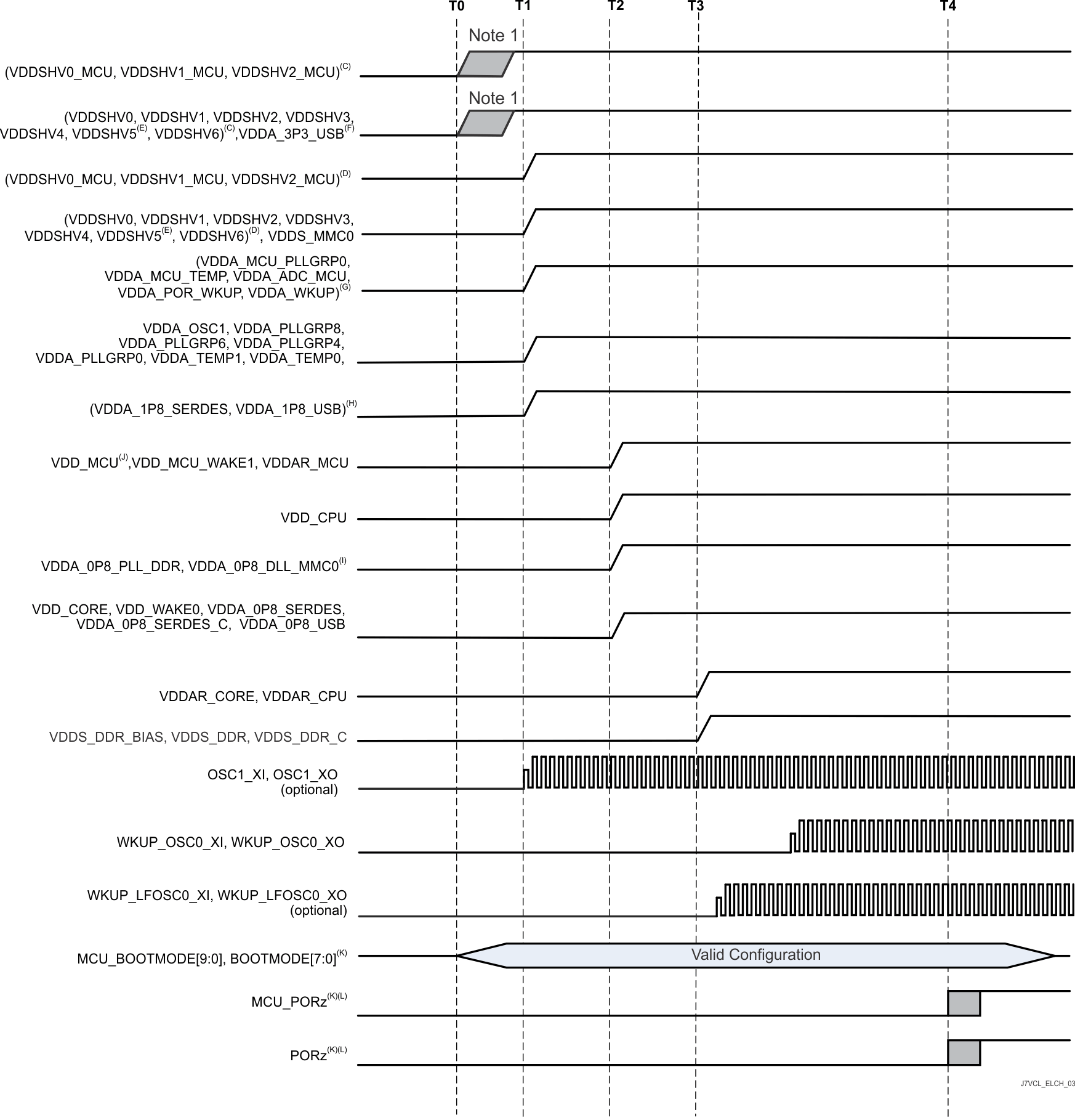
AM68A AM68 Isolated MCU and
          Main Domains, Primary Power-Up Sequence
T1Time stamp markers:
  • T0 – All 3.3-V voltages start supply ramp-up to VOPR MIN. (0 ms)
  • T1 – All 1.8-V voltages start supply ramp-up to VOPR MIN. (2 ms)
  • T2 – All core voltages start supply ramp-up to VOPR MIN. (3 ms)
  • T3 – All RAM array voltages start supply ramp-up to VOPR MIN. (4 ms)
  • T4 – OSC1 is stable and PORz/MCU_PORz are de-asserted to release processor from reset. (13 ms)
Any MCU or Main dual voltage IO supplies (VDDSHVn_MCU or VDDSHVn) being supplied by 3.3 V to support 3.3-V digital interfaces. A few supplies could have varying start times between T0 to T1 due to PDN designs using different power resources with varying turn-on & ramp-up time delays.
Any MCU or Main dual voltage IO supplies (VDDSHVn_MCU or VDDSHVn) being supplied by 1.8 V to support 1.8-V digital interfaces. When eMMC memories are used, Main 1.8-V supplies could have delayed start times that aligns to T3 due to PDN designs grouping supplies with VDD_MMC0.
VDDSHV5 supports MMC1 signaling for SD memory cards. If compliant UHS-I SD card operation is needed, then an independent, dual voltage (3.3 V/1.8 V) power source and rail are required. The start of ramp-up to 3.3 V will be same as other 3.3-V domains as shown. If SD card is not needed or standard data rates with fixed 3.3-V operation is acceptable, then supply can be grouped with digital IO 3.3-V power rail. If a SD card is capable of operating with fixed 1.8 V, then supply can be grouped with digital IO 1.8-V power rail.
VDDA_3P3_USB is 3.3-V analog supply used for USB 2.0 differential interface signaling. A low noise, analog supply is recommended to provide best signal integrity for USB data eye mask compliance. The start of ramp-up to 3.3 V will be same as other 3.3-V domains as shown. If USB interface is not needed or data bit errors can be tolerated, then supply can be grouped with 3.3-V digital IO power rail either directly or through a supply filter.
VDDA_1P8_<clk/pll/ana> are 1.8-V analog domains supporting clock oscillator, PLL and analog circuitry needing a low noise supply for optimal performance. It is not recommended to combine digital VDDSHVn_MCU and VDDSHVn IO domains since high frequency switching noise could negatively impact jitter performance of clock, PLL and DLL signals. Combining analog VDDA_1p8_<phy> domains should be avoided but if grouped, then in-line ferrite bead supply filtering is required.
VDDA_1P8_<phy> are 1.8-V analog domains supporting multiple serial PHY interfaces. A low noise, analog supply is recommended to provide best signal integrity, interface performance and spec compliance. If any of these interfaces are not needed, data bit errors or non-compliant operation can be tolerated, then domains can be grouped with digital IO 1.8-V power rail either directly or through an in-line supply filter is allowed.
VDDA_0P8_<dll/pll> are 0.8-V analog domains supporting PLL and DLL circuitry needing a low noise supply for optimal performance. It is not recommended to combine these domains with any other 0.8-V domains since high frequency switching noise could negatively impact jitter performance of PLL and DLL signals.
VDD_MCU is a digital voltage domain with a wide operational voltage range enabling it to be grouped either with VDDAR_MCU domain or with VDD_CORE; for the “Isolated MCU and Main Domains Power-Up Sequencing,” VDD_MCU can be grouped with VDDAR_MCU; VDD_MCU must be ramped-up before T2. If VDDAR_MCU is not grouped with VDD_MCU, it must be ramped at T3.
Minimum set-up and hold times shown with respect to MCU_PORz and PORz asserting high to latch MCU_BOOTMODEn (referenced to MCU_VDDSHV0) and BOOTMODEn (reference to VDDSHV2) settings into registers during power up sequence.
Minimum elapsed time from crystal oscillator circuitry being energized (VDDA_OSC1 at T1) until stable clock frequency is reached depends upon on crystal oscillator, capacitor parameters and PCB parasitic values. A conservative 10 ms elapsed time defined by (T4 – T1) time stamps is shown. This could be reduced depending upon customer’s clock circuit (that is, crystal oscillator or clock generator) and PCB designs.
Figure 6-5 Isolated MCU and Main Domains, Primary Power-Up Sequence