SPRSP91B February 2023 – December 2024 AM68 , AM68A
PRODUCTION DATA
- 1
- 1 Features
- 2 Applications
- 3 Description
- 4 Device Comparison
-
5 Terminal Configuration and Functions
- 5.1 Pin Diagrams
- 5.2 Pin Attributes
- 5.3
Signal Descriptions
- 13
- 5.3.1 ADC
- 5.3.2 DDRSS
- 5.3.3 GPIO
- 5.3.4 I2C
- 5.3.5 I3C
- 5.3.6 MCAN
- 5.3.7 MCSPI
- 5.3.8 UART
- 5.3.9 MDIO
- 5.3.10 CPSW2G
- 5.3.11 ECAP
- 5.3.12 EQEP
- 5.3.13 EPWM
- 5.3.14 USB
- 5.3.15 Display Port
- 5.3.16 Hyperlink
- 5.3.17 PCIE
- 5.3.18 SERDES
- 5.3.19 DSI
- 5.3.20 CSI
- 5.3.21 MCASP
- 5.3.22 DMTIMER
- 5.3.23 CPTS
- 5.3.24 DSS
- 5.3.25 GPMC
- 5.3.26 MMC
- 5.3.27 OSPI
- 5.3.28 Hyperbus
- 5.3.29 Emulation and Debug
- 5.3.30 System and Miscellaneous
- 5.3.31 Power
- 5.4 Connection for Unused Pins
-
6 Specifications
- 6.1 Absolute Maximum Ratings
- 6.2 ESD Ratings
- 6.3 Recommended Operating Conditions
- 6.4 Power-On-Hour (POH) Limits
- 6.5 Operating Performance Points
- 6.6
Electrical Characteristics
- 6.6.1 I2C, Open-Drain, Fail-Safe (I2C OD FS) Electrical Characteristics
- 6.6.2 Fail-Safe Reset (FS Reset) Electrical Characteristics
- 6.6.3 HFOSC/LFOSC Electrical Characteristics
- 6.6.4 eMMCPHY Electrical Characteristics
- 6.6.5 SDIO Electrical Characteristics
- 6.6.6 CSI2/DSI D-PHY Electrical Characteristics
- 6.6.7 ADC12B Electrical Characteristics
- 6.6.8 LVCMOS Electrical Characteristics
- 6.6.9 USB2PHY Electrical Characteristics
- 6.6.10 SerDes 2-L-PHY/4-L-PHY Electrical Characteristics
- 6.6.11 UFS M-PHY Electrical Characteristics
- 6.6.12 eDP/DP AUX-PHY Electrical Characteristics
- 6.6.13 DDR0 Electrical Characteristics
- 6.7 VPP Specifications for One-Time Programmable (OTP) eFuses
- 6.8 Thermal Resistance Characteristics
- 6.9 Temperature Sensor Characteristics
- 6.10
Timing and Switching Characteristics
- 6.10.1 Timing Parameters and Information
- 6.10.2
Power Supply Sequencing
- 6.10.2.1 Power Supply Slew Rate Requirement
- 6.10.2.2 Combined MCU and Main Domains Power- Up Sequencing
- 6.10.2.3 Combined MCU and Main Domains Power- Down Sequencing
- 6.10.2.4 Isolated MCU and Main Domains Power- Up Sequencing
- 6.10.2.5 Isolated MCU and Main Domains Power- Down Sequencing
- 6.10.2.6 Independent MCU and Main Domains, Entry and Exit of MCU Only Sequencing
- 6.10.2.7 Independent MCU and Main Domains, Entry and Exit of DDR Retention State
- 6.10.2.8 Independent MCU and Main Domains, Entry and Exit of GPIO Retention Sequencing
- 6.10.3 System Timing
- 6.10.4
Clock Specifications
- 6.10.4.1 Input and Output Clocks / Oscillators
- 6.10.4.2 Output Clocks
- 6.10.4.3 PLLs
- 6.10.4.4 Module and Peripheral Clocks Frequencies
- 6.10.5
Peripherals
- 6.10.5.1 ATL
- 6.10.5.2
CPSW2G
- 6.10.5.2.1 CPSW2G MDIO Interface Timings
- 6.10.5.2.2 CPSW2G RMII Timings
- 6.10.5.2.3
CPSW2G RGMII Timings
- 6.10.5.2.3.1 RGMII[x]_RXC Timing Requirements – RGMII Mode
- 6.10.5.2.3.2 CPSW2G Timing Requirements for RGMII[x]_RD[3:0], and RGMII[x]_RCTL – RGMII Mode
- 6.10.5.2.3.3 CPSW2G RGMII[x]_TXC Switching Characteristics – RGMII Mode
- 6.10.5.2.3.4 RGMII[x]_TD[3:0], and RGMII[x]_TX_CTL Switching Characteristics – RGMII Mode
- 6.10.5.3 CSI-2
- 6.10.5.4 DDRSS
- 6.10.5.5 DSS
- 6.10.5.6 eCAP
- 6.10.5.7 EPWM
- 6.10.5.8 eQEP
- 6.10.5.9 GPIO
- 6.10.5.10 GPMC
- 6.10.5.11 HyperBus
- 6.10.5.12 I2C
- 6.10.5.13 I3C
- 6.10.5.14 MCAN
- 6.10.5.15 MCASP
- 6.10.5.16 MCSPI
- 6.10.5.17 MMCSD
- 6.10.5.18 CPTS
- 6.10.5.19 OSPI
- 6.10.5.20 PCIE
- 6.10.5.21 Timers
- 6.10.5.22 UART
- 6.10.5.23 USB
- 6.10.6 Emulation and Debug
- 7 Detailed Description
-
8 Applications,
Implementation, and Layout
- 8.1 Device Connection and Layout Fundamentals
- 8.2 Peripheral- and Interface-Specific Design Information
- 9 Device and Documentation Support
- 10Revision History
- 11Mechanical, Packaging, and Orderable Information
Package Options
Refer to the PDF data sheet for device specific package drawings
Mechanical Data (Package|Pins)
- ALZ|770
Thermal pad, mechanical data (Package|Pins)
Orderable Information
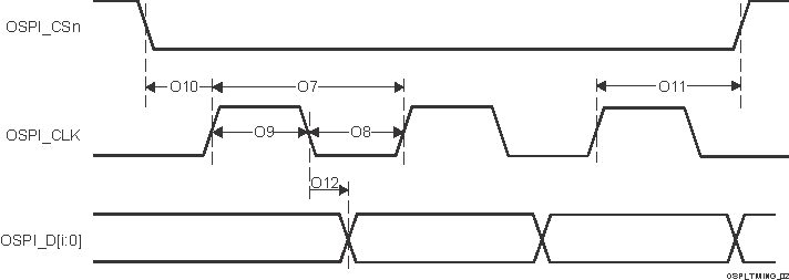
| NO. | PARAMETER | DESCRIPTION | MODE | MIN | MAX | UNIT |
|---|---|---|---|---|---|---|
| O7 | tc(CLK) | Cycle time, CLK | 1.8V | 7 | ns | |
| 3.3V | 7.5 | ns | ||||
| O8 | tw(CLKL) | Pulse duration, CLK low | ((0.475P(1)) - 0.3) | ns | ||
| O9 | Pulse duration, CLK high | ((0.475P(1)) - 0.3) | ns | |||
| O10 | ttd(CSn-CLK) | Delay time, CSn active edge to CLK rising edge | 1.8V | ((0.475P(1)) + (0.975M(2)R(4)) + (0.028TD(5)) - 1) | ((0.525P(1)) + (1.025M(2)R(4)) + (0.055TD(5)) + 1) | ns |
| 3.3V | ((0.475P(1)) + (0.975M(2)R(4)) + (0.028TD(5)) - 1) | ((0.525P(1)) + (1.025M(2)R(4)) + (0.055TD(5)) + 1) | ns | |||
| O11 | td(CLK-CSn) | Delay time, CLK rising edge to CSn inactive edge | 1.8V | ((0.475P(1)) + (0.975N(3)R(4)) - (0.055TD(5)) - 1) | ((0.525P(1)) + (1.025N(3)R(4)) - (0.028TD(5)) + 1) | ns |
| 3.3V | ((0.475P(1)) + (0.975N(3)R(4)) - (0.055TD(5)) - 1) | ((0.525P(1)) + (1.025N(3)R(4)) - (0.028TD(5)) + 1) | ns | |||
| O12 | td(CLK-D) | Delay time, CLK active edge to D[i:0] transition(6) | 1.8V | –1.16 | 1.25 | ns |
| 3.3V | –1.33 | 1.51 | ns |
(1) P = CLK cycle time
= SCLK period
(2) M = OSPI_DEV_DELAY_REG[D_INIT_FLD]
(3) N =
OSPI_DEV_DELAY_REG[D_AFTER_FLD]
(4) R = refclk
(5) TD = PHY_CONFIG_TX_DLL_DELAY_FLD
(6) i in [i:0] = 7 for OSPI0, i in [i:0] = 3 for OSPI1
 Figure 6-104 OSPI
Switching Characteristics – SDR
Figure 6-104 OSPI
Switching Characteristics – SDRSection 6.10.5.19.1.2.3, Section 6.10.5.19.1.2.1, Section 6.10.5.19.1.2.2, Section 6.10.5.19.1.2.2, and Figure 6-103 presents timing requirements for OSPI DDR and SDR Mode.