SPRSP92D February 2023 – December 2024 AM69 , AM69A
PRODUCTION DATA
- 1
- 1 Features
- 2 Applications
- 3 Description
- 4 Device Comparison
-
5 Terminal Configuration and Functions
- 5.1 Pin Diagrams
- 5.2 Pin Attributes
- 5.3
Signal Descriptions
- 13
- 5.3.1 ADC
- 5.3.2 DDRSS
- 5.3.3 GPIO
- 5.3.4 I2C
- 5.3.5 I3C
- 5.3.6 MCAN
- 5.3.7 MCSPI
- 5.3.8 UART
- 5.3.9 MDIO
- 5.3.10 UFS
- 5.3.11 CPSW2G
- 5.3.12 SGMII
- 5.3.13 ECAP
- 5.3.14 EQEP
- 5.3.15 EPWM
- 5.3.16 USB
- 5.3.17 Display Port
- 5.3.18 PCIE
- 5.3.19 SERDES
- 5.3.20 DSI
- 5.3.21 CSI
- 5.3.22 MCASP
- 5.3.23 DMTIMER
- 5.3.24 CPTS
- 5.3.25 DSS
- 5.3.26 GPMC
- 5.3.27 MMC
- 5.3.28 OSPI
- 5.3.29 Hyperbus
- 5.3.30 Emulation and Debug
- 5.3.31 System and Miscellaneous
- 5.3.32 Power
- 5.4 Pin Connectivity Requirements
-
6 Specifications
- 6.1 Absolute Maximum Ratings
- 6.2 ESD Ratings
- 6.3 Power-On-Hour (POH) Limits
- 6.4 Recommended Operating Conditions
- 6.5 Operating Performance Points
- 6.6
Electrical Characteristics
- 6.6.1 I2C, Open-Drain, Fail-Safe (I2C OD FS) Electrical Characteristics
- 6.6.2 Fail-Safe Reset (FS Reset) Electrical Characteristics
- 6.6.3 HFOSC/LFOSC Electrical Characteristics
- 6.6.4 eMMCPHY Electrical Characteristics
- 6.6.5 SDIO Electrical Characteristics
- 6.6.6 CSI2/DSI D-PHY Electrical Characteristics
- 6.6.7 ADC12B Electrical Characteristics
- 6.6.8 LVCMOS Electrical Characteristics
- 6.6.9 USB2PHY Electrical Characteristics
- 6.6.10 SerDes 2-L-PHY/4-L-PHY Electrical Characteristics
- 6.6.11 UFS M-PHY Electrical Characteristics
- 6.6.12 eDP/DP AUX-PHY Electrical Characteristics
- 6.6.13 DDR0 Electrical Characteristics
- 6.7 VPP Specifications for One-Time Programmable (OTP) eFuses
- 6.8 Thermal Resistance Characteristics
- 6.9 Temperature Sensor Characteristics
- 6.10
Timing and Switching Characteristics
- 6.10.1 Timing Parameters and Information
- 6.10.2
Power Supply Sequencing
- 6.10.2.1 Power Supply Slew Rate Requirement
- 6.10.2.2 Combined MCU and Main Domains Power- Up Sequencing
- 6.10.2.3 Combined MCU and Main Domains Power- Down Sequencing
- 6.10.2.4 Isolated MCU and Main Domains Power- Up Sequencing
- 6.10.2.5 Isolated MCU and Main Domains Power- Down Sequencing
- 6.10.2.6 Independent MCU and Main Domains, Entry and Exit of MCU Only Sequencing
- 6.10.2.7 Independent MCU and Main Domains, Entry and Exit of DDR Retention State
- 6.10.2.8 Independent MCU and Main Domains, Entry and Exit of GPIO Retention Sequencing
- 6.10.3 System Timing
- 6.10.4
Clock Specifications
- 6.10.4.1 Input and Output Clocks / Oscillators
- 6.10.4.2 Output Clocks
- 6.10.4.3 PLLs
- 6.10.4.4 Module and Peripheral Clocks Frequencies
- 6.10.5
Peripherals
- 6.10.5.1 ATL
- 6.10.5.2
CPSW2G
- 6.10.5.2.1 CPSW2G MDIO Interface Timings
- 6.10.5.2.2 CPSW2G RMII Timings
- 6.10.5.2.3
CPSW2G RGMII Timings
- 6.10.5.2.3.1 RGMII[x]_RXC Timing Requirements – RGMII Mode
- 6.10.5.2.3.2 CPSW2G Timing Requirements for RGMII[x]_RD[3:0], and RGMII[x]_RCTL – RGMII Mode
- 6.10.5.2.3.3 CPSW2G RGMII[x]_TXC Switching Characteristics – RGMII Mode
- 6.10.5.2.3.4 RGMII[x]_TD[3:0], and RGMII[x]_TX_CTL Switching Characteristics – RGMII Mode
- 6.10.5.3 CSI-2
- 6.10.5.4 DDRSS
- 6.10.5.5 DSS
- 6.10.5.6 eCAP
- 6.10.5.7 EPWM
- 6.10.5.8 eQEP
- 6.10.5.9 GPIO
- 6.10.5.10 GPMC
- 6.10.5.11 HyperBus
- 6.10.5.12 I2C
- 6.10.5.13 I3C
- 6.10.5.14 MCAN
- 6.10.5.15 MCASP
- 6.10.5.16 MCSPI
- 6.10.5.17 MMCSD
- 6.10.5.18 CPTS
- 6.10.5.19 OSPI
- 6.10.5.20 OLDI
- 6.10.5.21 PCIE
- 6.10.5.22 Timers
- 6.10.5.23 UART
- 6.10.5.24 USB
- 6.10.6 Emulation and Debug
-
7 Detailed Description
- 7.1 Overview
- 7.2 Functional Block Diagram
- 7.3 Processor Subsystems
- 7.4 Accelerators and Coprocessors
- 7.5
Other Subsystems
- 7.5.1 MSMC
- 7.5.2 NAVSS
- 7.5.3 PDMA Controller
- 7.5.4 Power Supply
- 7.5.5
Peripherals
- 7.5.5.1 ADC
- 7.5.5.2 ATL
- 7.5.5.3 CSI
- 7.5.5.4 CPSW2G
- 7.5.5.5 CPSW9G
- 7.5.5.6 DCC
- 7.5.5.7 DDRSS
- 7.5.5.8 DSS
- 7.5.5.9 eCAP
- 7.5.5.10 EPWM
- 7.5.5.11 ELM
- 7.5.5.12 ESM
- 7.5.5.13 eQEP
- 7.5.5.14 GPIO
- 7.5.5.15 GPMC
- 7.5.5.16 Hyperbus
- 7.5.5.17 I2C
- 7.5.5.18 I3C
- 7.5.5.19 MCAN
- 7.5.5.20 MCASP
- 7.5.5.21 MCRC Controller
- 7.5.5.22 MCSPI
- 7.5.5.23 MMC/SD
- 7.5.5.24 OSPI
- 7.5.5.25 PCIE
- 7.5.5.26 SerDes
- 7.5.5.27 WWDT
- 7.5.5.28 Timers
- 7.5.5.29 UART
- 7.5.5.30 USB
- 7.5.5.31 UFS
- 8 Applications, Implementation, and Layout
- 9 Device Connection and Layout Fundamentals
- 10Peripheral- and Interface-Specific Design Information
- 11Device and Documentation Support
- 12Revision History
- 13Mechanical, Packaging, and Orderable Information
Package Options
Refer to the PDF data sheet for device specific package drawings
Mechanical Data (Package|Pins)
- ALY|1414
Thermal pad, mechanical data (Package|Pins)
Orderable Information
10.2.2 External Board Loopback
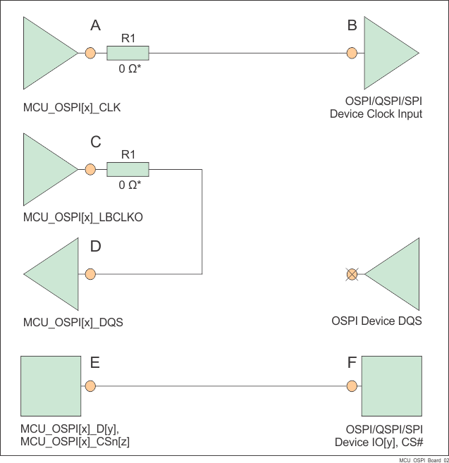
- The MCU_OSPI[x]_CLK output signal must be connected to the CLK pin of the flash device
- The MCU_OSPI[x]_LBCLKO output signal must be looped back into the MCU_OSPI[x]_DQS input
- The signal propagation delay from the MCU_OSPI[x]_CLK pin to the flash device CLK input pin (A to B) should be approximately equal to half of the signal propagation delay from the MCU_OPSI[x]_LBCLKO pin to the MCU_OSPI[x]_DQS pin ((C to D)/2). See the note below.
- The signal propagation delay from the MCU_OSPI[x]_CLK pin to the flash device CLK input pin (A to B) must be approximately equal to the signal propagation delay of the control and data signals between the flash device and the SoC device (E to F, or F to E)
- 50 Ω PCB routing is recommended along with series terminations, as shown in Figure 10-2
- Propagation delays and matching:
- A to B = E to F = (C to D) / 2
- Matching skew: < 60 ps
Note:
The OSPI Board Loopback Hold time requirement (described in OSPI) is larger than the Hold time provided by a typical flash device. Therefore, the length of MCU_OPSI[x]_LBCLKO pin to the MCU_OSPI[x]_DQS pin (C to D) can be shortened to compensate.

* 0 Ω resistor (R1), located as close as possible to the MCU_OSPI[x]_CLK and MCU_OSPI[x]_LBCLKO pins, is a placeholder for fine tuning, if needed.
Figure 10-2 OSPI Interface High Level Schematic