SPRSP92D February 2023 – December 2024 AM69 , AM69A
PRODUCTION DATA
- 1
- 1 Features
- 2 Applications
- 3 Description
- 4 Device Comparison
-
5 Terminal Configuration and Functions
- 5.1 Pin Diagrams
- 5.2 Pin Attributes
- 5.3
Signal Descriptions
- 13
- 5.3.1 ADC
- 5.3.2 DDRSS
- 5.3.3 GPIO
- 5.3.4 I2C
- 5.3.5 I3C
- 5.3.6 MCAN
- 5.3.7 MCSPI
- 5.3.8 UART
- 5.3.9 MDIO
- 5.3.10 UFS
- 5.3.11 CPSW2G
- 5.3.12 SGMII
- 5.3.13 ECAP
- 5.3.14 EQEP
- 5.3.15 EPWM
- 5.3.16 USB
- 5.3.17 Display Port
- 5.3.18 PCIE
- 5.3.19 SERDES
- 5.3.20 DSI
- 5.3.21 CSI
- 5.3.22 MCASP
- 5.3.23 DMTIMER
- 5.3.24 CPTS
- 5.3.25 DSS
- 5.3.26 GPMC
- 5.3.27 MMC
- 5.3.28 OSPI
- 5.3.29 Hyperbus
- 5.3.30 Emulation and Debug
- 5.3.31 System and Miscellaneous
- 5.3.32 Power
- 5.4 Pin Connectivity Requirements
-
6 Specifications
- 6.1 Absolute Maximum Ratings
- 6.2 ESD Ratings
- 6.3 Power-On-Hour (POH) Limits
- 6.4 Recommended Operating Conditions
- 6.5 Operating Performance Points
- 6.6
Electrical Characteristics
- 6.6.1 I2C, Open-Drain, Fail-Safe (I2C OD FS) Electrical Characteristics
- 6.6.2 Fail-Safe Reset (FS Reset) Electrical Characteristics
- 6.6.3 HFOSC/LFOSC Electrical Characteristics
- 6.6.4 eMMCPHY Electrical Characteristics
- 6.6.5 SDIO Electrical Characteristics
- 6.6.6 CSI2/DSI D-PHY Electrical Characteristics
- 6.6.7 ADC12B Electrical Characteristics
- 6.6.8 LVCMOS Electrical Characteristics
- 6.6.9 USB2PHY Electrical Characteristics
- 6.6.10 SerDes 2-L-PHY/4-L-PHY Electrical Characteristics
- 6.6.11 UFS M-PHY Electrical Characteristics
- 6.6.12 eDP/DP AUX-PHY Electrical Characteristics
- 6.6.13 DDR0 Electrical Characteristics
- 6.7 VPP Specifications for One-Time Programmable (OTP) eFuses
- 6.8 Thermal Resistance Characteristics
- 6.9 Temperature Sensor Characteristics
- 6.10
Timing and Switching Characteristics
- 6.10.1 Timing Parameters and Information
- 6.10.2
Power Supply Sequencing
- 6.10.2.1 Power Supply Slew Rate Requirement
- 6.10.2.2 Combined MCU and Main Domains Power- Up Sequencing
- 6.10.2.3 Combined MCU and Main Domains Power- Down Sequencing
- 6.10.2.4 Isolated MCU and Main Domains Power- Up Sequencing
- 6.10.2.5 Isolated MCU and Main Domains Power- Down Sequencing
- 6.10.2.6 Independent MCU and Main Domains, Entry and Exit of MCU Only Sequencing
- 6.10.2.7 Independent MCU and Main Domains, Entry and Exit of DDR Retention State
- 6.10.2.8 Independent MCU and Main Domains, Entry and Exit of GPIO Retention Sequencing
- 6.10.3 System Timing
- 6.10.4
Clock Specifications
- 6.10.4.1 Input and Output Clocks / Oscillators
- 6.10.4.2 Output Clocks
- 6.10.4.3 PLLs
- 6.10.4.4 Module and Peripheral Clocks Frequencies
- 6.10.5
Peripherals
- 6.10.5.1 ATL
- 6.10.5.2
CPSW2G
- 6.10.5.2.1 CPSW2G MDIO Interface Timings
- 6.10.5.2.2 CPSW2G RMII Timings
- 6.10.5.2.3
CPSW2G RGMII Timings
- 6.10.5.2.3.1 RGMII[x]_RXC Timing Requirements – RGMII Mode
- 6.10.5.2.3.2 CPSW2G Timing Requirements for RGMII[x]_RD[3:0], and RGMII[x]_RCTL – RGMII Mode
- 6.10.5.2.3.3 CPSW2G RGMII[x]_TXC Switching Characteristics – RGMII Mode
- 6.10.5.2.3.4 RGMII[x]_TD[3:0], and RGMII[x]_TX_CTL Switching Characteristics – RGMII Mode
- 6.10.5.3 CSI-2
- 6.10.5.4 DDRSS
- 6.10.5.5 DSS
- 6.10.5.6 eCAP
- 6.10.5.7 EPWM
- 6.10.5.8 eQEP
- 6.10.5.9 GPIO
- 6.10.5.10 GPMC
- 6.10.5.11 HyperBus
- 6.10.5.12 I2C
- 6.10.5.13 I3C
- 6.10.5.14 MCAN
- 6.10.5.15 MCASP
- 6.10.5.16 MCSPI
- 6.10.5.17 MMCSD
- 6.10.5.18 CPTS
- 6.10.5.19 OSPI
- 6.10.5.20 OLDI
- 6.10.5.21 PCIE
- 6.10.5.22 Timers
- 6.10.5.23 UART
- 6.10.5.24 USB
- 6.10.6 Emulation and Debug
-
7 Detailed Description
- 7.1 Overview
- 7.2 Functional Block Diagram
- 7.3 Processor Subsystems
- 7.4 Accelerators and Coprocessors
- 7.5
Other Subsystems
- 7.5.1 MSMC
- 7.5.2 NAVSS
- 7.5.3 PDMA Controller
- 7.5.4 Power Supply
- 7.5.5
Peripherals
- 7.5.5.1 ADC
- 7.5.5.2 ATL
- 7.5.5.3 CSI
- 7.5.5.4 CPSW2G
- 7.5.5.5 CPSW9G
- 7.5.5.6 DCC
- 7.5.5.7 DDRSS
- 7.5.5.8 DSS
- 7.5.5.9 eCAP
- 7.5.5.10 EPWM
- 7.5.5.11 ELM
- 7.5.5.12 ESM
- 7.5.5.13 eQEP
- 7.5.5.14 GPIO
- 7.5.5.15 GPMC
- 7.5.5.16 Hyperbus
- 7.5.5.17 I2C
- 7.5.5.18 I3C
- 7.5.5.19 MCAN
- 7.5.5.20 MCASP
- 7.5.5.21 MCRC Controller
- 7.5.5.22 MCSPI
- 7.5.5.23 MMC/SD
- 7.5.5.24 OSPI
- 7.5.5.25 PCIE
- 7.5.5.26 SerDes
- 7.5.5.27 WWDT
- 7.5.5.28 Timers
- 7.5.5.29 UART
- 7.5.5.30 USB
- 7.5.5.31 UFS
- 8 Applications, Implementation, and Layout
- 9 Device Connection and Layout Fundamentals
- 10Peripheral- and Interface-Specific Design Information
- 11Device and Documentation Support
- 12Revision History
- 13Mechanical, Packaging, and Orderable Information
Package Options
Refer to the PDF data sheet for device specific package drawings
Mechanical Data (Package|Pins)
- ALY|1414
Thermal pad, mechanical data (Package|Pins)
Orderable Information
6.10.4.1.3 Auxiliary OSC1 Internal Oscillator Clock Source
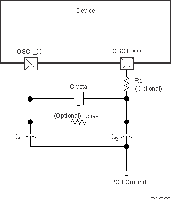
Figure 6-28 shows the recommended crystal circuit. All discrete components used to implement the oscillator circuit should be placed as close as possible to the OSC1_XI and OSC1_XO pins.
 Figure 6-28 OSC1 Crystal Implementation
The crystal must be in the fundamental mode of operation and parallel resonant. Table 6-23 summarizes the required electrical constraints.
| PARAMETER | MIN | TYP | MAX | UNIT | |||
|---|---|---|---|---|---|---|---|
| Fxtal | Crystal Parallel Resonance Frequency | 19.2 | 27 | MHz | |||
| Fxtal | Crystal Frequency Stability and Tolerance | Ethernet RGMII and RMII not used | ±100 | ppm | |||
| Ethernet RGMII and RMII using derived clock | ±50 | ||||||
| CL1+PCBXI | Capacitance of CL1 + CPCBXI | 12 | 24 | pF | |||
| CL2+PCBXO | Capacitance of CL2 + CPCBXO | 12 | 24 | pF | |||
| CL | Crystal Load Capacitance | 6 | 12 | pF | |||
| Cshunt | Crystal Circuit Shunt Capacitance | 19.2MHz ≤ Fxtal ≤ 20MHz | ESRxtal ≤ 30 Ω | 7 | pF | ||
| 30 Ω ≤ ESRxtal ≤ 80 Ω | 5 | pF | |||||
| 80 Ω ≤ ESRxtal ≤ 100 Ω | 3 | pF | |||||
| 20MHz ≤ Fxtal ≤ 24.576MHz | ESRxtal ≤ 30 Ω | 7 | pF | ||||
| 30 Ω ≤ ESRxtal ≤ 60 Ω | 5 | pF | |||||
| 60 Ω ≤ ESRxtal ≤ 80 Ω | 3 | pF | |||||
| Not Supported: 80 Ω ≤ ESRxtal | – | ||||||
| 24.576MHz ≤ Fxtal ≤ 25MHz | ESRxtal ≤ 30 Ω | 7 | pF | ||||
| 30 Ω ≤ ESRxtal ≤ 50 Ω | 5 | pF | |||||
| 50 Ω ≤ ESRxtal ≤ 80 Ω | 3 | pF | |||||
| Not Supported: 80 Ω ≤ ESRxtal | – | ||||||
| 25MHz ≤ Fxtal ≤ 27MHz | ESRxtal ≤ 30 Ω | 7 | pF | ||||
| 30 Ω ≤ ESRxtal ≤ 50 Ω | 5 | pF | |||||
| Not Supported: 50 Ω ≤ ESRxtal | – | ||||||
| ESRxtal | Crystal Effective Series Resistance | 100 | Ω | ||||
When selecting a crystal, the system design must consider the temperature and aging characteristics of a based on the worst case environment and expected life expectancy of the system.
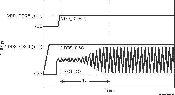
Table 6-24 details the switching characteristics of the oscillator and the requirements of the input clock.
| PARAMETER | PACKAGE | MIN | TYP | MAX | UNIT | ||
|---|---|---|---|---|---|---|---|
| CXI | XI Capacitance | ALY | 1.989 | pF | |||
| CXO | XO Capacitance | ALY | 1.971 | pF | |||
| CXIXO | XI to XO Mutual Capacitance | ALY | 0.01 | pF | |||
| ts | Start-up Time | 9.5(1) | ms | ||||
| PARAMETER | PACKAGE | MIN | TYP | MAX | UNIT | ||
| CXI | XI Capacitance | ALY | 1.989 | pF | |||
| AND | 2.548 | pF | |||||
| CXO | XO Capacitance | ALY | 1.971 | pF | |||
| AND | 2.878 | pF | |||||
| CXIXO | XI to XO Mutual Capacitance | ALY | 0.01 | pF | |||
| AND | 0.01 | pF | |||||
| ts | Start-up Time | 9.5(1) | ms | ||||
 Figure 6-29 OSC1 Start-up Time