SBASAZ0A August 2024 – December 2024 AMC0136
PRODUCTION DATA
- 1
- 1 Features
- 2 Applications
- 3 Description
- 4 Pin Configuration and Functions
- 5 Specifications
- 6 Detailed Description
- 7 Application and Implementation
- 8 Device and Documentation Support
- 9 Revision History
- 10Mechanical, Packaging, and Orderable Information
Package Options
Mechanical Data (Package|Pins)
- DEN|8
Thermal pad, mechanical data (Package|Pins)
Orderable Information
7.2.2.2 Bitstream Filtering
The modulator generates a bitstream that is processed by a digital filter to obtain a digital word similar to a conversion result of a conventional analog-to-digital converter (ADC). Equation 2 represents a sinc3-type filter, which is a very simple filter that is built with minimal effort and hardware.
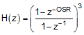
This filter provides the best output performance at the lowest hardware size (count of digital gates) for a second-order modulator. All characterization in this document is also done with a sinc3 filter with an oversampling ratio (OSR) of 256 and an output word width of 16 bits.
An example code for implementing a sinc3 filter in an FPGA is discussed in the Combining the ADS1202 with an FPGA Digital Filter for Current Measurement in Motor Control Applications application note, available for download at www.ti.com.
For modulator output bitstream filtering, a device from TI's C2000 or Sitara microcontroller families is recommended. These families support multichannel dedicated hardwired filter structures that significantly simplify system level design by offering two filtering paths per channel: one path provides high-accuracy results for the control loop and the other provides a fast-response path for overcurrent detection.
A delta sigma modulator filter calculator is available for download at www.ti.com that aids in the filter design and selecting the right OSR and filter order to achieve the desired output resolution and filter response time.