SBAS562B April 2012 – December 2019 AMC1100
PRODUCTION DATA.
- 1 Features
- 2 Applications
- 3 Description
- 4 Revision History
- 5 Pin Configuration and Functions
-
6 Specifications
- 6.1 Absolute Maximum Ratings
- 6.2 ESD Ratings
- 6.3 Recommended Operating Conditions
- 6.4 Thermal Information
- 6.5 Power Ratings
- 6.6 Insulation Specifications
- 6.7 Safety-Related Certifications
- 6.8 Safety Limiting Values
- 6.9 Electrical Characteristics
- 6.10 Insulation Characteristics Curves
- 6.11 Typical Characteristics
- 7 Detailed Description
- 8 Application and Implementation
- 9 Power Supply Recommendations
- 10Layout
- 11Device and Documentation Support
- 12Mechanical, Packaging, and Orderable Information
Package Options
Mechanical Data (Package|Pins)
Thermal pad, mechanical data (Package|Pins)
- DUB|8
Orderable Information
11.1.1.1 Isolation Glossary
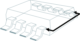
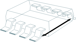
Creepage Distance: The shortest path between two conductive input-to-output leads measured along the surface of the insulation. The shortest distance path is found around the end of the package body.

Clearance: The shortest distance between two conductive input-to-output leads measured through air (line of sight).

Input-to-Output Barrier Capacitance: The total capacitance between all input terminals connected together, and all output terminals connected together.
Input-to-Output Barrier Resistance: The total resistance between all input terminals connected together, and all output terminals connected together.
Primary Circuit: An internal circuit directly connected to an external supply mains or other equivalent source that supplies the primary circuit electric power.
Secondary Circuit: A circuit with no direct connection to primary power that derives its power from a separate isolated source.
Comparative Tracking Index (CTI): CTI is an index used for electrical insulating materials. It is defined as the numerical value of the voltage that causes failure by tracking during standard testing. Tracking is the process that produces a partially conducting path of localized deterioration on or through the surface of an insulating material as a result of the action of electric discharges on or close to an insulation surface. The higher CTI value of the insulating material, the smaller the minimum creepage distance.
Generally, insulation breakdown occurs either through the material, over its surface, or both. Surface failure may arise from flashover or from the progressive insulation surface degradation by small localized sparks. Such sparks result from a surface film of a conducting contaminant breaking on the insulation. The resulting break in the leakage current produces an overvoltage at the site of the discontinuity, and an electric spark is generated. These sparks often cause carbonization on insulation material and lead to a carbon track between points of different potential. This process is known as tracking.