SBASAN9 September 2023 AMC130M02
PRODUCTION DATA
- 1
- 1 Features
- 2 Applications
- 3 Description
- 4 Revision History
- 5 Pin Configuration and Functions
-
6 Specifications
- 6.1 Absolute Maximum Ratings
- 6.2 ESD Ratings
- 6.3 Recommended Operating Conditions
- 6.4 Thermal Information
- 6.5 Insulation Specifications
- 6.6 Safety-Related Certifications
- 6.7 Safety Limiting Values
- 6.8 Electrical Characteristics
- 6.9 Timing Requirements
- 6.10 Switching Characteristics
- 6.11 Timing Diagrams
- 6.12 Typical Characteristics
- 7 Parameter Measurement Information
-
8 Detailed Description
- 8.1 Overview
- 8.2 Functional Block Diagram
- 8.3
Feature Description
- 8.3.1 Isolated DC/DC Converter
- 8.3.2 High-Side Current Drive Capability
- 8.3.3 Isolation Channel Signal Transmission
- 8.3.4 Input ESD Protection Circuitry
- 8.3.5 Input Multiplexer
- 8.3.6 Programmable Gain Amplifier (PGA)
- 8.3.7 Voltage Reference
- 8.3.8 Internal Test Signals
- 8.3.9 Clocking and Power Modes
- 8.3.10 ΔΣ Modulator
- 8.3.11 Digital Filter
- 8.3.12 Channel Phase Calibration
- 8.3.13 Calibration Registers
- 8.3.14 Register Map CRC
- 8.3.15 General-Purpose Digital Output (GPO)
- 8.4 Device Functional Modes
- 8.5
Programming
- 8.5.1
Serial Interface
- 8.5.1.1 Chip Select (CS)
- 8.5.1.2 Serial Data Clock (SCLK)
- 8.5.1.3 Serial Data Input (DIN)
- 8.5.1.4 Serial Data Output (DOUT)
- 8.5.1.5 Data Ready (DRDY)
- 8.5.1.6 Conversion Synchronization or System Reset (SYNC/RESET)
- 8.5.1.7 SPI Communication Frames
- 8.5.1.8 SPI Communication Words
- 8.5.1.9 Short SPI Frames
- 8.5.1.10 Communication Cyclic Redundancy Check (CRC)
- 8.5.1.11 SPI Timeout
- 8.5.2 ADC Conversion Data Format
- 8.5.3 Commands
- 8.5.4 ADC Output Buffer and FIFO Buffer
- 8.5.5 Collecting Data for the First Time or After a Pause in Data Collection
- 8.5.1
Serial Interface
- 8.6 AMC130M02 Registers
- 9 Application and Implementation
- 10Device and Documentation Support
- 11Mechanical, Packaging, and Orderable Information
Package Options
Mechanical Data (Package|Pins)
- DFM|20
Thermal pad, mechanical data (Package|Pins)
Orderable Information
8.3.12 Channel Phase Calibration
The AMC130M02 allows fine adjustment of the sample phase between channels by using channel phase calibration. This feature is helpful when different channels are measuring the outputs of different types of sensors that have different phase responses. For example, in power metrology applications, voltage can be measured by a voltage divider, whereas current is measured using a current transformer that exhibits a phase difference between the input and output signals. The differences in phase between the voltage and current measurement must be compensated to measure the power and related parameters accurately.
The phase setting of the different channels is configured by the PHASEn[9:0] bits in the CHn_CFG register corresponding to the channel whose phase adjustment is desired. The register value is a 10-bit, two's-complement value corresponding to the number of modulator clock cycles of phase offset compared to a reference phase of zero degrees.
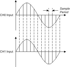
The mechanism for achieving phase adjustment derives from the ΔΣ architecture. The ΔΣ modulator produces samples continuously at the modulator frequency, fMOD. These samples are filtered and decimated to the output data rate by the digital filter. The ratio between fMOD and the data rate is the oversampling ratio (OSR). Each conversion result corresponds to an OSR number of modulator samples provided to the digital filter. When the different channels of the AMC130M02 have no programmed phase offset between them, the modulator clock cycles corresponding to the conversion results of the different channels are aligned in the time domain. Figure 8-11 shows an example scenario where the voltage input to channel 1 has no phase offset from channel 0.
 Figure 8-11 Two Channel Outputs With Equal Phase Settings
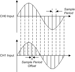
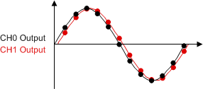
However, the sample period of one channel can be shifted with respect to another. If the inputs to both channels are sinusoids of the same frequency and the samples for these channels are retrieved by the host at the same time, the effect is that the phase of the channel with the modified sample period appears shifted. Figure 8-12 shows how the period corresponding to the samples are shifted between channels. Figure 8-13 illustrates how the samples appear as having generated a phase shift when retrieved by the host.
 Figure 8-12 Channel 1 With a Positive Sample Phase Shift With Respect to Channel 0
 Figure 8-13 Channels 1 and 0 From the Perspective of the Host
The valid setting range is from –OSR / 2 to (OSR / 2) – 1, except for OSRs greater than 1024, where the phase calibration setting is limited to –512 to 511. If a value outside of –OSR / 2 and (OSR / 2) – 1 is programmed, the device internally clips the value to the nearest limit. For example, if the OSR setting is programmed to 128 and the PHASEn[9:0] bits are programmed to 0001100100b corresponding to 100 modulator clock cycles, the device sets the phase of the channel to 63 because that value is the upper limit of phase calibration for that OSR setting. Table 8-6 gives the range of phase calibration settings for various OSR settings.
| OSR SETTING | PHASE OFFSET RANGE (tMOD) | PHASEn[9:0] BITS RANGE |
|---|---|---|
| 64 | –32 to 31 | 11 1110 0000b to 00 0001 1111b |
| 128 | –64 to 63 | 11 1100 0000b to 00 0011 1111b |
| 256 | –128 to 127 | 11 1000 0000b to 00 0111 1111b |
| 512 | –256 to 255 | 11 0000 0000b to 00 1111 1111b |
| 1024 | –512 to 511 | 10 0000 0000b to 01 1111 1111b |
| 2048 | –512 to 511 | 10 0000 0000b to 01 1111 1111b |
| 4096 | –512 to 511 | 10 0000 0000b to 01 1111 1111b |
| 8192 | –512 to 511 | 10 0000 0000b to 01 1111 1111b |
| 16384 | –512 to 511 | 10 0000 0000b to 01 1111 1111b |
Follow these steps to create a phase shift larger than half the sample period for OSRs less than 2048:
- Create a phase shift corresponding to an integer number of sample periods by modifying the indices between channel data in software
- Use the phase calibration function of the AMC130M02 to create the remaining fractional sample period phase shift
The phase calibration settings of the channels affect the timing of the data-ready interrupt signal, DRDY. See the Data Ready (DRDY) section for more details regarding how phase calibration affects the DRDY signal.