SBASA56 September 2023 AMC131M02
PRODUCTION DATA
- 1
- 1 Features
- 2 Applications
- 3 Description
- 4 Revision History
- 5 Pin Configuration and Functions
-
6 Specifications
- 6.1 Absolute Maximum Ratings
- 6.2 ESD Ratings
- 6.3 Recommended Operating Conditions
- 6.4 Thermal Information
- 6.5 Insulation Specifications
- 6.6 Safety-Related Certifications
- 6.7 Safety Limiting Values
- 6.8 Electrical Characteristics
- 6.9 Timing Requirements
- 6.10 Switching Characteristics
- 6.11 Timing Diagrams
- 6.12 Typical Characteristics
- 7 Parameter Measurement Information
-
8 Detailed Description
- 8.1 Overview
- 8.2 Functional Block Diagram
- 8.3
Feature Description
- 8.3.1 Isolated DC/DC Converter
- 8.3.2 High-Side Current Drive Capability
- 8.3.3 Isolation Channel Signal Transmission
- 8.3.4 Input ESD Protection Circuitry
- 8.3.5 Input Multiplexer
- 8.3.6 Programmable Gain Amplifier (PGA)
- 8.3.7 Voltage Reference
- 8.3.8 Internal Test Signals
- 8.3.9 Clocking and Power Modes
- 8.3.10 ΔΣ Modulator
- 8.3.11 Digital Filter
- 8.3.12 Channel Phase Calibration
- 8.3.13 Calibration Registers
- 8.3.14 Register Map CRC
- 8.3.15 General-Purpose Digital Output (GPO)
- 8.4 Device Functional Modes
- 8.5
Programming
- 8.5.1
Serial Interface
- 8.5.1.1 Chip Select (CS)
- 8.5.1.2 Serial Data Clock (SCLK)
- 8.5.1.3 Serial Data Input (DIN)
- 8.5.1.4 Serial Data Output (DOUT)
- 8.5.1.5 Data Ready (DRDY)
- 8.5.1.6 Conversion Synchronization or System Reset (SYNC/RESET)
- 8.5.1.7 SPI Communication Frames
- 8.5.1.8 SPI Communication Words
- 8.5.1.9 Short SPI Frames
- 8.5.1.10 Communication Cyclic Redundancy Check (CRC)
- 8.5.1.11 SPI Timeout
- 8.5.2 ADC Conversion Data
- 8.5.3 Commands
- 8.5.4 ADC Output Buffer and FIFO Buffer
- 8.5.5 Collecting Data for the First Time or After a Pause in Data Collection
- 8.5.1
Serial Interface
- 8.6 AMC131M02 Registers
- 9 Application and Implementation
- 10Device and Documentation Support
- 11Mechanical, Packaging, and Orderable Information
Package Options
Mechanical Data (Package|Pins)
- DFM|20
Thermal pad, mechanical data (Package|Pins)
Orderable Information
8.5.3.2 RESET (0000 0000 0001 0001)
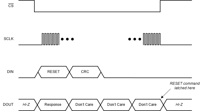
The RESET command resets the ADC to the register defaults. The command is latched by the device at the end of the frame. A reset occurs immediately after the command is latched. The host must wait for tREGACQ after reset before communicating with the device to make sure the registers have assumed the default settings. The device sends an acknowledgment of FF23h when the ADC is properly reset. The device responds with 0011h if the command word is sent but the frame is not completed, and therefore, the device is not reset. See the RESET Command section for more information regarding the operation of the reset command. Figure 8-24 illustrates a properly sent RESET command frame.
 Figure 8-24 RESET Command Frame