SBAS994B September 2023 – September 2023 AMC131M03
PRODUCTION DATA
- 1
- 1 Features
- 2 Applications
- 3 Description
- 4 Revision History
- 5 Pin Configuration and Functions
-
6 Specifications
- 6.1 Absolute Maximum Ratings
- 6.2 ESD Ratings
- 6.3 Recommended Operating Conditions
- 6.4 Thermal Information
- 6.5 Insulation Specifications
- 6.6 Safety-Related Certifications
- 6.7 Safety Limiting Values
- 6.8 Electrical Characteristics
- 6.9 Timing Requirements
- 6.10 Switching Characteristics
- 6.11 Timing Diagrams
- 6.12 Typical Characteristics
- 7 Parameter Measurement Information
-
8 Detailed Description
- 8.1 Overview
- 8.2 Functional Block Diagram
- 8.3
Feature Description
- 8.3.1 Isolated DC/DC Converter
- 8.3.2 High-Side Current Drive Capability
- 8.3.3 Isolation Channel Signal Transmission
- 8.3.4 Input ESD Protection Circuitry
- 8.3.5 Input Multiplexer
- 8.3.6 Programmable Gain Amplifier (PGA)
- 8.3.7 Voltage Reference
- 8.3.8 Internal Test Signals
- 8.3.9 Clocking and Power Modes
- 8.3.10 ΔΣ Modulator
- 8.3.11 Digital Filter
- 8.3.12 Channel Phase Calibration
- 8.3.13 Calibration Registers
- 8.3.14 Register Map CRC
- 8.3.15 Temperature Sensor
- 8.3.16 General-Purpose Digital Output (GPO)
- 8.4 Device Functional Modes
- 8.5
Programming
- 8.5.1
Serial Interface
- 8.5.1.1 Chip Select (CS)
- 8.5.1.2 Serial Data Clock (SCLK)
- 8.5.1.3 Serial Data Input (DIN)
- 8.5.1.4 Serial Data Output (DOUT)
- 8.5.1.5 Data Ready (DRDY)
- 8.5.1.6 Conversion Synchronization or System Reset (SYNC/RESET)
- 8.5.1.7 SPI Communication Frames
- 8.5.1.8 SPI Communication Words
- 8.5.1.9 Short SPI Frames
- 8.5.1.10 Communication Cyclic Redundancy Check (CRC)
- 8.5.1.11 SPI Timeout
- 8.5.2 ADC Conversion Data
- 8.5.3 Commands
- 8.5.4 ADC Output Buffer and FIFO Buffer
- 8.5.5 Collecting Data for the First Time or After a Pause in Data Collection
- 8.5.1
Serial Interface
- 8.6 AMC131M03 Registers
- 9 Application and Implementation
- 10Device and Documentation Support
- 11Mechanical, Packaging, and Orderable Information
Package Options
Mechanical Data (Package|Pins)
- DFM|20
Thermal pad, mechanical data (Package|Pins)
Orderable Information
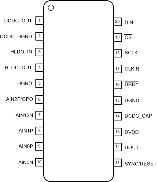
5 Pin Configuration and Functions
 Figure 5-1 DFM Package,20-Pin SOIC(Top View)
Table 5-1 Pin Functions
| PIN | TYPE | DESCRIPTION(1) | |||
|---|---|---|---|---|---|
| NO. | NAME | ||||
| 1 | DCDC_OUT | Supply | High-side output of the DC/DC converter. Connect this pin to the HLDO_IN pin.(2) | ||
| 2 | DCDC_HGND | Supply | High-side ground reference for the DC/DC converter. Connect this pin to the HGND pin.(2) | ||
| 3 | HLDO_IN | Supply | Input of the high-side low-dropout (LDO) regulator. Connect this pin to the DCDC_OUT pin.(2) | ||
| 4 | HLDO_OUT | Supply | Output of the high-side LDO.(2) | ||
| 5 | HGND | Supply | High-side analog signal ground. Connect this pin to the DCDC_HGND pin. | ||
| 6 | AIN2P/GPO | Analog input | Positive analog input 2, or general-purpose output. | ||
| 7 | AIN12N | Analog input | Negative analog input 1 and 2. | ||
| 8 | AIN1P | Analog input | Positive analog input 1. | ||
| 9 | AIN0P(3) | Analog input | Positive analog input 0. | ||
| 10 | AIN0N(3) | Analog input | Negative analog input 0. | ||
| 11 | SYNC/RESET | Digital input | Conversion synchronization or system reset; active low. | ||
| 12 | DOUT | Digital output | Serial data output. | ||
| 13 | DVDD | Supply | Low-side analog and digital power supply.(2) | ||
| 14 | DCDC_CAP | Supply | Low-side input of the DC/DC converter, internally connected to the output of the primary-side LDO.(2) | ||
| 15 | DGND | Supply | Low-side analog and digital ground.(2) | ||
| 16 | DRDY | Digital output | Data ready; active low. | ||
| 17 | CLKIN | Digital input | Main clock input. | ||
| 18 | SCLK | Digital input | Serial data clock. | ||
| 19 | CS | Digital input | Chip select; active low. | ||
| 20 | DIN | Digital input | Serial data input. | ||
(1) See the Unused Inputs and Outputs section for details on how to connect unused pins.
(2) See the Power Supply
Recommendations section for power-supply decoupling recommendations.
(3) Use
AIN0P and AIN0N for the measurement with the most stringent precision
requirements.