SBAS994B September 2023 – September 2023 AMC131M03
PRODUCTION DATA
- 1
- 1 Features
- 2 Applications
- 3 Description
- 4 Revision History
- 5 Pin Configuration and Functions
-
6 Specifications
- 6.1 Absolute Maximum Ratings
- 6.2 ESD Ratings
- 6.3 Recommended Operating Conditions
- 6.4 Thermal Information
- 6.5 Insulation Specifications
- 6.6 Safety-Related Certifications
- 6.7 Safety Limiting Values
- 6.8 Electrical Characteristics
- 6.9 Timing Requirements
- 6.10 Switching Characteristics
- 6.11 Timing Diagrams
- 6.12 Typical Characteristics
- 7 Parameter Measurement Information
-
8 Detailed Description
- 8.1 Overview
- 8.2 Functional Block Diagram
- 8.3
Feature Description
- 8.3.1 Isolated DC/DC Converter
- 8.3.2 High-Side Current Drive Capability
- 8.3.3 Isolation Channel Signal Transmission
- 8.3.4 Input ESD Protection Circuitry
- 8.3.5 Input Multiplexer
- 8.3.6 Programmable Gain Amplifier (PGA)
- 8.3.7 Voltage Reference
- 8.3.8 Internal Test Signals
- 8.3.9 Clocking and Power Modes
- 8.3.10 ΔΣ Modulator
- 8.3.11 Digital Filter
- 8.3.12 Channel Phase Calibration
- 8.3.13 Calibration Registers
- 8.3.14 Register Map CRC
- 8.3.15 Temperature Sensor
- 8.3.16 General-Purpose Digital Output (GPO)
- 8.4 Device Functional Modes
- 8.5
Programming
- 8.5.1
Serial Interface
- 8.5.1.1 Chip Select (CS)
- 8.5.1.2 Serial Data Clock (SCLK)
- 8.5.1.3 Serial Data Input (DIN)
- 8.5.1.4 Serial Data Output (DOUT)
- 8.5.1.5 Data Ready (DRDY)
- 8.5.1.6 Conversion Synchronization or System Reset (SYNC/RESET)
- 8.5.1.7 SPI Communication Frames
- 8.5.1.8 SPI Communication Words
- 8.5.1.9 Short SPI Frames
- 8.5.1.10 Communication Cyclic Redundancy Check (CRC)
- 8.5.1.11 SPI Timeout
- 8.5.2 ADC Conversion Data
- 8.5.3 Commands
- 8.5.4 ADC Output Buffer and FIFO Buffer
- 8.5.5 Collecting Data for the First Time or After a Pause in Data Collection
- 8.5.1
Serial Interface
- 8.6 AMC131M03 Registers
- 9 Application and Implementation
- 10Device and Documentation Support
- 11Mechanical, Packaging, and Orderable Information
Package Options
Mechanical Data (Package|Pins)
- DFM|20
Thermal pad, mechanical data (Package|Pins)
Orderable Information
8.5.1.7 SPI Communication Frames
SPI communication on the AMC131M03 is performed in frames. Each SPI communication frame consists of several words. The word size is configurable as either 16, 24, or 32 bits by programming the WLENGTH[1:0] bits in the MODE register.
The interface is full duplex, meaning that the interface is capable of transmitting data on DOUT while simultaneously receiving data on DIN. The input frame that the host sends on DIN always begins with a command. The first word on the output frame that the device transmits on DOUT always begins with the response to the command that was sent in the previous input frame.
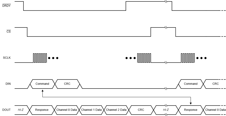
The number of words in a command depends on the command provided. For most commands, there are five words in a frame. On DIN, the host provides the command, the command CRC if input CRC is enabled or a word of zeros if input CRC is disabled, and three additional words of zeros. Simultaneously on DOUT, the device outputs the response from the previous frame command, three words of ADC data representing the three ADC channels, and a CRC word. If one or several of the ADC channels are disabled, this frame structure of five words still applies, and the data of disabled channels reads all zeros. Figure 8-24 shows a typical command frame structure.
 Figure 8-24 Typical
Communication Frame
Figure 8-24 Typical
Communication FrameThere are some commands that require more than five words. In the case of a read register (RREG) command where multiple registers are read, the response to the command contains the acknowledgment of the command followed by the register contents requested, which can require a larger frame depending on how many registers are read. See the RREG section for more details on the RREG command.
In the case of a write register (WREG) command where multiple registers are written, the frame extends to accommodate the additional data. See the WREG section for more details on the WREG command.
See the Commands section for a list of all valid commands and the corresponding responses on the AMC131M03.
Under special circumstances, a data frame can be shortened by the host. See the Short SPI Frames section for more information about artificially shortening communication frames.