SBAS994B September 2023 – September 2023 AMC131M03
PRODUCTION DATA
- 1
- 1 Features
- 2 Applications
- 3 Description
- 4 Revision History
- 5 Pin Configuration and Functions
-
6 Specifications
- 6.1 Absolute Maximum Ratings
- 6.2 ESD Ratings
- 6.3 Recommended Operating Conditions
- 6.4 Thermal Information
- 6.5 Insulation Specifications
- 6.6 Safety-Related Certifications
- 6.7 Safety Limiting Values
- 6.8 Electrical Characteristics
- 6.9 Timing Requirements
- 6.10 Switching Characteristics
- 6.11 Timing Diagrams
- 6.12 Typical Characteristics
- 7 Parameter Measurement Information
-
8 Detailed Description
- 8.1 Overview
- 8.2 Functional Block Diagram
- 8.3
Feature Description
- 8.3.1 Isolated DC/DC Converter
- 8.3.2 High-Side Current Drive Capability
- 8.3.3 Isolation Channel Signal Transmission
- 8.3.4 Input ESD Protection Circuitry
- 8.3.5 Input Multiplexer
- 8.3.6 Programmable Gain Amplifier (PGA)
- 8.3.7 Voltage Reference
- 8.3.8 Internal Test Signals
- 8.3.9 Clocking and Power Modes
- 8.3.10 ΔΣ Modulator
- 8.3.11 Digital Filter
- 8.3.12 Channel Phase Calibration
- 8.3.13 Calibration Registers
- 8.3.14 Register Map CRC
- 8.3.15 Temperature Sensor
- 8.3.16 General-Purpose Digital Output (GPO)
- 8.4 Device Functional Modes
- 8.5
Programming
- 8.5.1
Serial Interface
- 8.5.1.1 Chip Select (CS)
- 8.5.1.2 Serial Data Clock (SCLK)
- 8.5.1.3 Serial Data Input (DIN)
- 8.5.1.4 Serial Data Output (DOUT)
- 8.5.1.5 Data Ready (DRDY)
- 8.5.1.6 Conversion Synchronization or System Reset (SYNC/RESET)
- 8.5.1.7 SPI Communication Frames
- 8.5.1.8 SPI Communication Words
- 8.5.1.9 Short SPI Frames
- 8.5.1.10 Communication Cyclic Redundancy Check (CRC)
- 8.5.1.11 SPI Timeout
- 8.5.2 ADC Conversion Data
- 8.5.3 Commands
- 8.5.4 ADC Output Buffer and FIFO Buffer
- 8.5.5 Collecting Data for the First Time or After a Pause in Data Collection
- 8.5.1
Serial Interface
- 8.6 AMC131M03 Registers
- 9 Application and Implementation
- 10Device and Documentation Support
- 11Mechanical, Packaging, and Orderable Information
Package Options
Mechanical Data (Package|Pins)
- DFM|20
Thermal pad, mechanical data (Package|Pins)
Orderable Information
8.5.5 Collecting Data for the First Time or After a Pause in Data Collection
Take special precaution when collecting data for the first time or when beginning to collect data again after a pause. As explained in the Collecting Data for the First Time or After a Pause in Data CollectionCollecting Data for the First Time or After a Pause in Data CollectionADC Output Buffer and FIFO BufferCollecting Data for the First Time or After a Pause in Data CollectionADC Output Buffer and FIFO Buffer section, the device contains a first-in-first-out (FIFO) buffer in addition to the ADC output buffer. When the host is reading each consecutive sample from the device, both buffers are updated each time new data are generated, so the DRDY flag in the STATUS register is cleared with each read. However, if data are not read for a period of time, previous samples can be lost as explained in the Collecting Data for the First Time or After a Pause in Data CollectionCollecting Data for the First Time or After a Pause in Data CollectionADC Output Buffer and FIFO BufferCollecting Data for the First Time or After a Pause in Data CollectionADC Output Buffer and FIFO Buffer section. Either strobe the SYNC/RESET pin to resynchronize conversions and clear the buffers, or quickly read two data packets when data are read for the first time or after a gap in reading data. This process ensures predictable DRDY pin behavior. See the SynchronizationSynchronizationSynchronizationSynchronizationSynchronization section for information about the synchronization feature. These methods do not need to be employed if each channel data is read for each output data period from when the ADC is enabled.
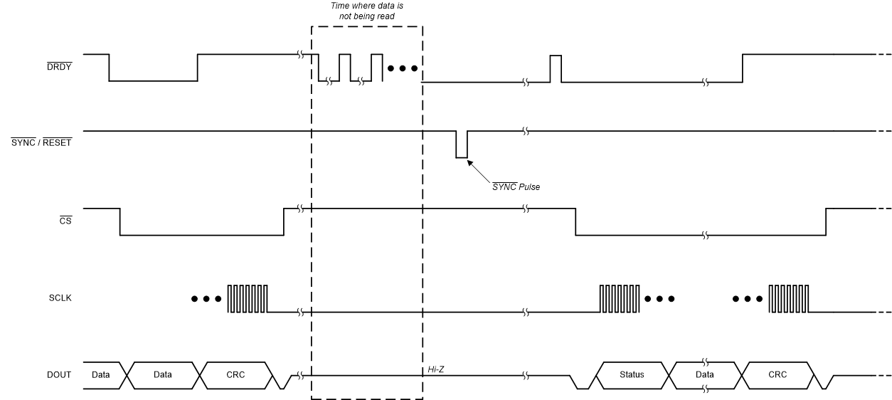
Figure 8-31 shows an example of how to collect data after a period of the ADC running, but where no data are being retrieved. In this instance, the SYNC/RESET pin clears the internal buffers and realigns the AMC131M03 output data with the host.
 Figure 8-31 Collecting Data After a Pause Using the
SYNC/RESET
Pin
Figure 8-31 Collecting Data After a Pause Using the
SYNC/RESET
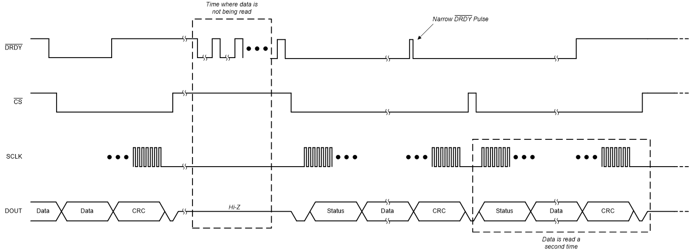
PinAnother functionally equivalent method for clearing the FIFO after a pause in collecting data is to begin by reading two samples in quick succession. Figure 8-32 shows this method. This example shows that when the DRDY_FMT bit in the MODE register is set to 0b, DRDY is a level output. There is a very narrow pulse on DRDY immediately after the first set of data are shifted out of the device. This pulse can be too narrow for some microcontrollers to detect. Therefore, do not rely upon this pulse but instead immediately read out the second data set after the first data set. The host operates synchronous to the device after the second word is read from the device.
 Figure 8-32 Collecting Data After a Pause by Reading Data
Twice