SBASA73A July 2020 – May 2021 AMC3301-Q1
PRODUCTION DATA
- 1 Features
- 2 Applications
- 3 Description
- 4 Revision History
- 5 Pin Configuration and Functions
-
6 Specifications
- 6.1 Absolute Maximum Ratings
- 6.2 ESD Ratings
- 6.3 Recommended Operating Conditions
- 6.4 Thermal Information
- 6.5 Power Ratings
- 6.6 Insulation Specifications
- 6.7 Safety-Related Certifications
- 6.8 Safety Limiting Values
- 6.9 Electrical Characteristics
- 6.10 Switching Characteristics
- 6.11 Timing Diagram
- 6.12 Insulation Characteristics Curves
- 6.13 Typical Characteristics
- 7 Detailed Description
- 8 Application and Implementation
- 9 Power Supply Recommendations
- 10Layout
- 11Device and Documentation Support
- 12Mechanical, Packaging, and Orderable Information
Package Options
Mechanical Data (Package|Pins)
- DWE|16
Thermal pad, mechanical data (Package|Pins)
Orderable Information
9 Power Supply Recommendations
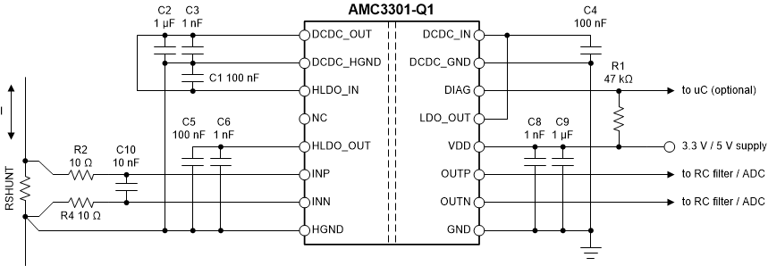
The AMC3301-Q1 is powered from the low-side power supply (VDD) with a nominal value of 3.3 V or 5 V. TI recommends a low-ESR decoupling capacitor of 1 nF (C8 in Figure 9-1) placed as close as possible to the VDD pin, followed by a 1-µF capacitor (C9) to filter this power-supply path.
The low-side of the DC/DC converter is decoupled with a low-ESR 100-nF capacitor (C4) positioned close to the device between the DCDC_IN and DCDC_GND pins. Use a 1-µF capacitor (C2) to decouple the high side in addition to a low-ESR, 1-nF capacitor (C3) placed as close as possible to the device and connected to the DCDC_OUT and DCDC_HGND pins.
For the high-side LDO, use low-ESR capacitors of 1-nF (C6), placed as close as possible to the AMC3301-Q1, followed by a 100-nF decoupling capacitor (C5).
The ground reference for the high-side (HGND) is derived from the terminal of the shunt resistor which is connected to the negative input (INN) of the device. For best DC accuracy, use a separate trace to make this connection instead of shorting HGND to INN directly at the device input. The high-side DC/DC ground terminal (DCDC_HGND) is shorted to HGND directly at the device pins.
 Figure 9-1 Decoupling the AMC3301-Q1
Capacitors must provide adequate effective capacitance under the applicable DC bias conditions they experience in the application. Multilayer ceramic capacitors (MLCC) typically exhibit only a fraction of their nominal capacitance under real-world conditions and this factor must be taken into consideration when selecting these capacitors. This problem is especially acute in low-profile capacitors, in which the dielectric field strength is higher than in taller components. Reputable capacitor manufacturers provide capacitance versus DC bias curves that greatly simplify component selection.
Table 9-1 lists components suitable for use with the AMC3301-Q1. This list is not exhaustive. Other components may exist that are equally suitable (or better), however these listed components have been validated during the development of the AMC3301-Q1.
| DESCRIPTION | PART NUMBER | MANUFACTURER | SIZE (EIA, L x W) | |
|---|---|---|---|---|
| VDD | ||||
| C8 | 1 nF ± 10%, X7R, 50 V | 12065C102KAT2A | AVX | 1206, 3.2 mm x 1.6 mm |
| C9 | 1 µF ± 10%, X7R, 25 V | 12063C105KAT2A | AVX | 1206, 3.2 mm x 1.6 mm |
| DC/DC CONVERTER | ||||
| C4 | 100 nF ± 10%, X7R, 50 V | C0603C104K5RACAUTO | Kemet | 0603, 1.6 mm x 0.8 mm |
| C3 | 1 nF ± 10%, X7R, 50 V | C0603C102K5RACTU | Kemet | 0603, 1.6 mm x 0.8 mm |
| C2 | 1 µF ± 10%, X7R, 25 V | CGA3E1X7R1E105K080AC | TDK | 0603, 1.6 mm x 0.8 mm |
| HLDO | ||||
| C1 | 100 nF ± 10%, X7R, 50 V | C0603C104K5RACAUTO | Kemet | 0603, 1.6 mm x 0.8 mm |
| C5 | 100 nF ± 5%, NP0, 50 V | C3216NP01H104J160AA | TDK | 1206, 3.2 mm x 1.6 mm |
| C6 | 1 nF ± 10%, X7R, 50 V | 12065C102KAT2A | AVX | 1206, 3.2 mm x 1.6 mm |