SBASB00 August 2024 AMC3306M25-Q1
PRODUCTION DATA
- 1
- 1 Features
- 2 Applications
- 3 Description
- 4 Pin Configuration and Functions
-
5 Specifications
- 5.1 Absolute Maximum Ratings
- 5.2 ESD Ratings
- 5.3 Recommended Operating Conditions
- 5.4 Thermal Information
- 5.5 Power Ratings
- 5.6 Insulation Specifications
- 5.7 Safety-Related Certifications
- 5.8 Safety Limiting Values
- 5.9 Electrical Characteristics
- 5.10 Switching Characteristics
- 5.11 Timing Diagrams
- 5.12 Insulation Characteristics Curves
- 5.13 Typical Characteristics
- 6 Detailed Description
- 7 Application and Implementation
- 8 Device and Documentation Support
- 9 Revision History
- 10Mechanical, Packaging, and Orderable Information
Package Options
Mechanical Data (Package|Pins)
- DWE|16
Thermal pad, mechanical data (Package|Pins)
Orderable Information
7.1.1 Digital Filter Usage
The modulator generates a bitstream that is required to be processed by a digital filter. This process obtains a digital word similar to a conversion result of a conventional analog-to-digital converter (ADC). A very simple filter, as shown in Equation 2, built with minimal effort and hardware, is a sinc3-type filter:
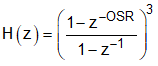
This filter provides the best output performance at the lowest hardware size (count of digital gates) for a second-order modulator. All characterization in this document is done with a 256 OSR sinc3 filter and a 16-bit output word width, unless otherwise noted. The measured effective number of bits (ENOB) as a function of the OSR is illustrated in Figure 7-3 of the Typical Application section.
A delta sigma modulator filter calculator is available for download at www.ti.com. This calculator aids in the filter design and correct OSR and filter-order selection to achieve the desired output resolution and filter response time.
The Combining the ADS1202 with an FPGA Digital Filter for Current Measurement in Motor Control Applications application note, available at www.ti.com, discusses an example code. This example code implements a sinc3 filter in an FPGA.