SBASB00 August 2024 AMC3306M25-Q1
PRODUCTION DATA
- 1
- 1 Features
- 2 Applications
- 3 Description
- 4 Pin Configuration and Functions
-
5 Specifications
- 5.1 Absolute Maximum Ratings
- 5.2 ESD Ratings
- 5.3 Recommended Operating Conditions
- 5.4 Thermal Information
- 5.5 Power Ratings
- 5.6 Insulation Specifications
- 5.7 Safety-Related Certifications
- 5.8 Safety Limiting Values
- 5.9 Electrical Characteristics
- 5.10 Switching Characteristics
- 5.11 Timing Diagrams
- 5.12 Insulation Characteristics Curves
- 5.13 Typical Characteristics
- 6 Detailed Description
- 7 Application and Implementation
- 8 Device and Documentation Support
- 9 Revision History
- 10Mechanical, Packaging, and Orderable Information
Package Options
Mechanical Data (Package|Pins)
- DWE|16
Thermal pad, mechanical data (Package|Pins)
Orderable Information
6.3.5 Isolated DC/DC Converter
The AMC3306M25-Q1 offers a fully integrated, isolated DC/DC converter with the following components(see the Functional Block Diagram section):
- Low-dropout regulator (LDO) on the low side to stabilize the supply voltage VDD that drives the low side of the converter. This circuit does not output a constant voltage and is not intended for driving any external load.
- Low-side full-bridge inverter and drivers.
- Laminate-based, air-core transformer for high immunity to magnetic fields.
- High-side full-bridge rectifier.
- High-side LDO to stabilize the output voltage of the DC/DC converter for high analog performance of the signal path. The high-side LDO outputs a constant voltage and optionally provides a limited amount of current to power external circuitry.
The DC/DC converter uses a spread-spectrum clock generation technique to reduce the spectral density of the electromagnetic radiation. The resonator frequency is synchronized to the ΔΣ modulator operation to minimize interference with data transmission and support high analog performance of the device.
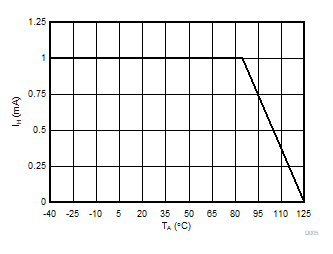
The architecture of the DC/DC converter is optimized to drive the high-side circuitry of the AMC3306M25-Q1. The DC/DC converter sources up to IH of additional DC current to power an optional active filter, preamplifier, or isolated comparator (such as the AMC23C12-Q1). As shown in Figure 6-6, IH is specified up to an ambient temperature of 85°C and derates linearly at higher temperatures.
 Figure 6-6 Derating of IH at
Ambient Temperatures >85°C