SBASA35B June 2020 – September 2024 AMC3330-Q1
PRODUCTION DATA
- 1
- 1 Features
- 2 Applications
- 3 Description
- 4 Pin Configuration and Functions
-
5 Specifications
- 5.1 Absolute Maximum Ratings
- 5.2 ESD Ratings
- 5.3 Recommended Operating Conditions
- 5.4 Thermal Information
- 5.5 Power Ratings
- 5.6 Insulation Specifications
- 5.7 Safety-Related Certifications
- 5.8 Safety Limiting Values
- 5.9 Electrical Characteristics
- 5.10 Switching Characteristics
- 5.11 Timing Diagram
- 5.12 Insulation Characteristics Curves
- 5.13 Typical Characteristics
- 6 Detailed Description
- 7 Application and Implementation
- 8 Device and Documentation Support
- 9 Revision History
- 10Mechanical, Packaging, and Orderable Information
Package Options
Mechanical Data (Package|Pins)
- DWE|16
Thermal pad, mechanical data (Package|Pins)
Orderable Information
6.3.2 Isolation Channel Signal Transmission
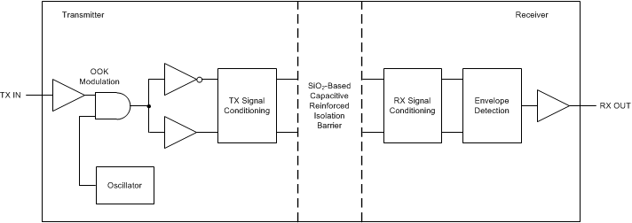
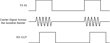
The AMC3330-Q1 uses an on-off keying (OOK) modulation scheme to transmit the modulator output-bitstream across the capacitive SiO2-based isolation barrier. Figure 6-1 shows the block diagram of an isolation channel. The transmitter modulates the bitstream at TX IN with an internally generated, 480-MHz carrier and sends a burst across the isolation barrier to represent a digital one and sends a no signal to represent the digital zero. The receiver demodulates the signal after advanced signal conditioning and produces the output. The symmetrical design of each isolation channel improves the common-mode transient immunity (CMTI) performance and reduces the radiated emissions caused by the high-frequency carrier.
 Figure 6-1 Block Diagram of an Isolation Channel
Figure 6-2 shows the concept of the on-off keying scheme.
 Figure 6-2 OOK-Based Modulation Scheme