SBASA35B June 2020 – September 2024 AMC3330-Q1
PRODUCTION DATA
- 1
- 1 Features
- 2 Applications
- 3 Description
- 4 Pin Configuration and Functions
-
5 Specifications
- 5.1 Absolute Maximum Ratings
- 5.2 ESD Ratings
- 5.3 Recommended Operating Conditions
- 5.4 Thermal Information
- 5.5 Power Ratings
- 5.6 Insulation Specifications
- 5.7 Safety-Related Certifications
- 5.8 Safety Limiting Values
- 5.9 Electrical Characteristics
- 5.10 Switching Characteristics
- 5.11 Timing Diagram
- 5.12 Insulation Characteristics Curves
- 5.13 Typical Characteristics
- 6 Detailed Description
- 7 Application and Implementation
- 8 Device and Documentation Support
- 9 Revision History
- 10Mechanical, Packaging, and Orderable Information
Package Options
Mechanical Data (Package|Pins)
- DWE|16
Thermal pad, mechanical data (Package|Pins)
Orderable Information
6.3.3 Analog Output
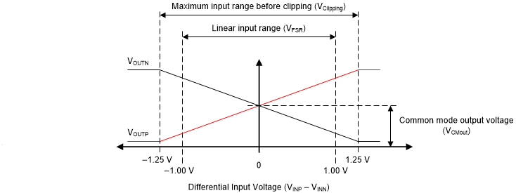
The AMC3330-Q1 offers a differential analog output comprised of the OUTP and OUTN pins. For differential input voltages (VINP – VINN) in the range from –1 V to 1 V, the device provides a linear response with a nominal gain of 2. For example, for a differential input voltage of 1 V, the differential output voltage (VOUTP – VOUTN) is 2 V. At zero input (INP shorted to INN), both pins output the same voltage, VCMout, as specified in the Electrical Characteristics table. For absolute differential input voltages greater than 1.0 V but less than 1.25 V, the differential output voltage continues to increase in magnitude but with reduced linearity performance. The outputs saturate as shown in Figure 6-3 if the differential input voltage exceeds the VClipping value.
 Figure 6-3 AMC3330-Q1 Output Behavior
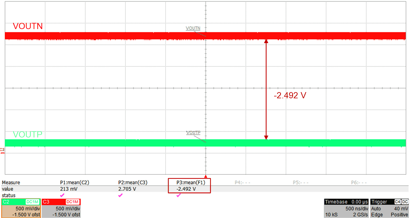
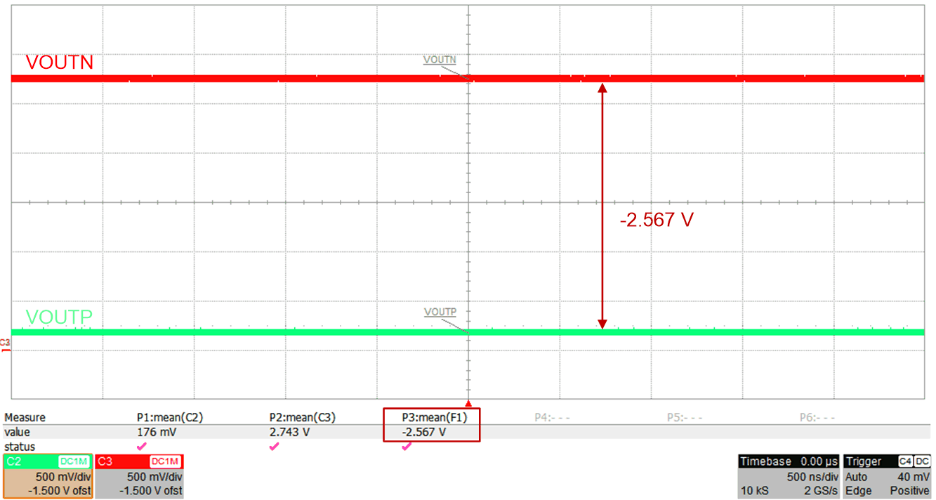
The AMC3330-Q1 provides a fail-safe output that simplifies diagnostics on system level. The fail-safe output is active when the integrated DC/DC converter or hgh-side LDO don't deliver the required supply voltage for the high-side of the device. Figure 6-4 and Figure 6-5 illustrate the fail-safe output of the AMC3330-Q1 that is a negative differential output voltage value that does not occur under normal operating conditions. Use the maximum VFAILSAFE voltage specified in the Electrical Characteristics table as a reference value for the fail-safe detection on system level.
 Figure 6-4 Typical Negative Clipping Output
of the AMC3330-Q1
 Figure 6-5 Typical Fail-Safe Output of the
AMC3330-Q1