SBASA34B June 2020 – August 2024 AMC3330
PRODUCTION DATA
- 1
- 1 Features
- 2 Applications
- 3 Description
- 4 Pin Configuration and Functions
-
5 Specifications
- 5.1 Absolute Maximum Ratings
- 5.2 ESD Ratings
- 5.3 Recommended Operating Conditions
- 5.4 Thermal Information
- 5.5 Power Ratings
- 5.6 Insulation Specifications
- 5.7 Safety-Related Certifications
- 5.8 Safety Limiting Values
- 5.9 Electrical Characteristics
- 5.10 Switching Characteristics
- 5.11 Timing Diagram
- 5.12 Insulation Characteristics Curves
- 5.13 Typical Characteristics
- 6 Detailed Description
- 7 Application and Implementation
- 8 Device and Documentation Support
- 9 Revision History
- 10Mechanical, Packaging, and Orderable Information
Package Options
Mechanical Data (Package|Pins)
- DWE|16
Thermal pad, mechanical data (Package|Pins)
Orderable Information
7.2.2.2 Differential to Single-Ended Output Conversion
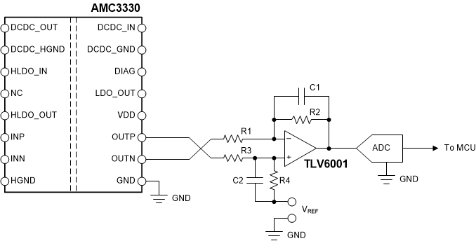
For systems using single-ended input ADCs to convert the analog output voltage into digital, Figure 7-3 shows an example of a TLV6001-based signal conversion and filter circuit. With R1 = R2 = R3 = R4, the output voltage equals (VOUTP – VOUTN) + VREF. Tailor the bandwidth of this filter stage to the bandwidth requirement of the system and use NP0-type capacitors for best performance. For most applications, R1 = R2 = R3 = R4 = 10 kΩ and C1 = C2 = 1000 pF yields good performance.
 Figure 7-3 Connecting
the AMC3330 Output to a Single-Ended Input ADC
Figure 7-3 Connecting
the AMC3330 Output to a Single-Ended Input ADCFor more information on the general procedure to design the filtering and driving stages of SAR ADCs, see the 18-Bit, 1MSPS Data Acquisition Block (DAQ) Optimized for Lowest Distortion and Noise and 18-Bit Data Acquisition Block (DAQ) Optimized for Lowest Power reference guides, available for download at www.ti.com.