-
AMC80 System Hardware Monitor with Two-Wire and SMBus Serial Interface
- 1 Features
- 2 Applications
- 3 Description
- 4 Revision History
- 5 Pin Configuration and Functions
- 6 Specifications
-
7 Detailed Description
- 7.1 Overview
- 7.2 Functional Block Diagram
- 7.3 Feature Description
- 7.4 Programming
- 7.5
Register Map
- 7.5.1 Configuration Register
- 7.5.2 Interrupt Status Registers
- 7.5.3 Interrupt Mask Registers
- 7.5.4 Fan Divisor/RST_OUT/OS Register
- 7.5.5 OS Configuration/Temperature Resolution Register
- 7.5.6 Conversion Rate Register
- 7.5.7 Voltage/Temperature Channel Disable Register
- 7.5.8 Input Mode Register
- 7.5.9 ADC Control Register
- 7.5.10 Conversion Rate Count Register
- 7.5.11 Value Ram Register
- 8 Application and Implementation
- 9 Device and Documentation Support
- 10Mechanical, Packaging, and Orderable Information
- IMPORTANT NOTICE
Package Options
Mechanical Data (Package|Pins)
- PW|24
Thermal pad, mechanical data (Package|Pins)
Orderable Information
AMC80 System Hardware Monitor with Two-Wire and SMBus Serial Interface
1 Features
- 10-Bit ADC With Seven Analog Inputs
- Fan-Speed Monitoring Inputs
- Input Range/Resolution:
- Default: 2.56 V/2.5 mV
- Programmable: VDD/6 mV
- Chassis Intrusion Detection Input
- Interrupt Alarms:
- Upper Over-Limit
- Lower Under-Limit
- Interrupt Status Register Input for External Temperature Sensors
- Shutdown Mode
- Programmable RST_OUT/OS
- Pin Compatible with LM96080 and LM80
- Package: 24-Pin TSSOP
2 Applications
- Communications Equipment
- Servers
- Industrial and Medical Equipment
- Storage Area Networks
- Set-Top Boxes
- Test and Measurement Equipment
3 Description
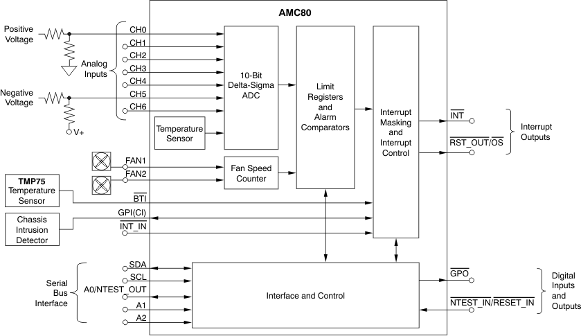
The AMC80 is a system hardware monitoring and control circuit that includes a seven-channel, 10-bit analog-to-digital converter (ADC), two programmable fan-speed monitors, and a two-wire interface. The AMC80 also includes programmable upper over-limit and lower under-limit alarms that activate when the programmed limits are exceeded.
The AMC80 can interface with both linear and digital temperature sensors. The 2.5-mV least significant bit (LSB) and 2.56-V input range can accept inputs from a linear sensor such as the TMP20. The BTI pin is used as an input from a digital sensor such as the TMP75. The AMC80 operates from a 3-V to 5.5-V supply voltage, has low supply current, and can be configured using a two-wire interface, thus making it ideal for a wide range of applications.
The AMC80 is available in a 24-lead TSSOP package and is fully specified over the –40°C to +125°C temperature range.
Device Information(1)
| PART NUMBER | PACKAGE | BODY SIZE (NOM) |
|---|---|---|
| AMC80 | TSSOP (24) | 7.80 mm × 4.40 mm |
- For all available packages, see the package option addendum at the end of the data sheet.
Simplified Schematic
4 Revision History
Changes from A Revision (January 2012) to B Revision
- Changed INT pin descriptionGo
- Added pins to input voltage range in Absolute Maximum Ratings tableGo
- Added ESD Ratings tableGo
- Added new note 1 to Timing Requirements tableGo
- Added Detailed Description sectionGo
- Added Application and Implementation sectionGo
- Added Device and Documentation Support sectionGo
Changes from * Revision (May 2011) to A Revision
5 Pin Configuration and Functions
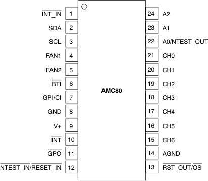
Pin Functions
6 Specifications
6.1 Absolute Maximum Ratings(1)
Over operating free-air temperature range, unless otherwise noted.6.2 ESD Ratings
| VALUE | UNIT | |||
|---|---|---|---|---|
| V(ESD) | Electrostatic discharge | Human-body model (HBM), per ANSI/ESDA/JEDEC JS-001(1) | ±2500 | V |
| Charged-device model (CDM), per JEDEC specification JESD22-C101(2) | ±1000 | |||
| Machine model (MM) | ±200 | |||
6.3 Recommended Operating Conditions
| MIN | NOM | MAX | UNIT | ||
|---|---|---|---|---|---|
| Supply voltage range, V+ | 3 | 5.5 | V | ||
| Input voltage range, VIN | –0.05 | (V+) + 0.05 | V | ||
| Operating temperature range, TA | –40 | 125 | °C | ||
6.4 Thermal Information
| THERMAL METRIC(1) | AMC80 | UNIT | |
|---|---|---|---|
| PW (TSSOP) | |||
| 24 PINS | |||
| RθJA | Junction-to-ambient thermal resistance | 100.72 | °C/W |
| RθJC(top) | Junction-to-case (top) thermal resistance | 31.4 | °C/W |
| RθJB | Junction-to-board thermal resistance | 54.7 | °C/W |
| ψJT | Junction-to-top characterization parameter | 1.0 | °C/W |
| ψJB | Junction-to-board characterization parameter | 54.2 | °C/W |
| RθJC(bot) | Junction-to-case (bottom) thermal resistance | N/A | °C/W |
6.5 Electrical Characteristics
At TA –40°C to +125°C and V+ = 3 V to 5.5 V, unless otherwise noted.| PARAMETER | TEST CONDITIONS | MIN | TYP | MAX | UNIT | |
|---|---|---|---|---|---|---|
| DIGITAL INPUTS | ||||||
| VIH | Input high voltage | 2 | V | |||
| VIL | Input low voltage | 0.8 | V | |||
| VHYS | Hysteresis voltage | V+ = 3.3 V | 0.23 | V | ||
| V+ = 5 V | 0.33 | V | ||||
| IIH | Input high current | VIH = V+, all pins except BTI | –1 | –0.005 | µA | |
| VIH = V+, BTI pin | –10 | –1 | µA | |||
| IIL | Input low current | VIL = 0 V, all pins except BTI | 0.005 | 1 | µA | |
| VIL = 0 V, V+ = 5.5 V, BTI pin | 2 | mA | ||||
| CIN | Input capacitance | 20 | pF | |||
| ANALOG INPUTS | ||||||
| VIN | Input voltage range | Default | 0 | 2.56 | V | |
| Programmable | 0 | V+ | V | |||
| IL-ON | Input leakage current (on) | ±0.005 | µA | |||
| IL-OFF | Input leakage current (off) | ±0.005 | µA | |||
| RIN | Input resistance | 2 | 10 | kΩ | ||
| DIGITAL OUTPUTS (A0/NTEST_OUT, INT) | ||||||
| VOH | Output high voltage | IOUT = 3 mA/5 mA, V+ = 3 V/4.5 V | 2.4 | V | ||
| VOL | Output low voltage | IOUT = 3 mA/5 mA, V+ = 3 V/4.5 V | 0.4 | V | ||
| DIGITAL OPEN-DRAIN OUTPUTS (GPO, RST_OUT/OS, GPI/CI, SDA) | ||||||
| VOL | Output low voltage | IOUT = 3 mA/5 mA, V+ = 3 V/4.5 V, all pins except SDA |
0.4 | V | ||
| IOUT = 4 mA, V+ = 3 V, SDA pin | 0.4 | |||||
| IOH | Output high current | VOUT = V+ | 0.005 | 1 | µA | |
| tw | Pulse duration | RST_OUT/OS, GPI/CI | 10 | 22.5 | ms | |
| SMBus | ||||||
| SMBus timeout(1) | 28 | 35 | ms | |||
| TEMPERATURE ERROR | ||||||
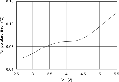
| TE | Temperature error | TA = –40°C to +125°C | ±3 | °C | ||
| TA = –25°C to +100°C | ±2 | °C | ||||
| TR | Temperature resolution | 0.0625 | °C | |||
| ANALOG-TO-DIGITAL CONVERTER | ||||||
| VR | Resolution | VIN = 2.56 V | 2.5 | mV | ||
| VIN = V+ | 6 | |||||
| DNL | Differential linearity | –1 | 1 | LSB(2) | ||
| ADCERR | Total unadjusted error(3) | –1% | 1% | |||
| PSRR | Power supply rejection ratio | ±0.0008% | ||||
| tC(4) | Total conversion time | 662 | 728 | 810 | ms | |
| FAN RPM-TO-DIGITAL CONVERTER | ||||||
| FANERR | Fan RPM error | –10% | 10% | |||
| fCLK | Internal clock frequency | 20.2 | 22.5 | 24.8 | kHz | |
| FANRPM | FAN1 and FAN2 nominal input RPM | Divisor = 1, fan count = 153 | 8800 | RPM | ||
| Divisor = 2, fan count = 153 | 4400 | |||||
| Divisor = 3, fan count = 153 | 2200 | |||||
| Divisor = 4, fan count = 153 | 1100 | |||||
| FSC | Full-scale count | 255 | Counts | |||
| POWER SUPPLY | ||||||
| V+ | Specified voltage range | 3 | 5.5 | V | ||
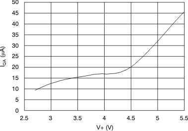
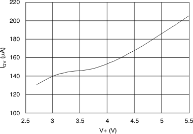
| IQA | Quiescent current, average | V+ = 5.5 V | 100 | µA | ||
| V+ = 3.8 V | 25 | |||||
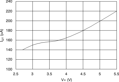
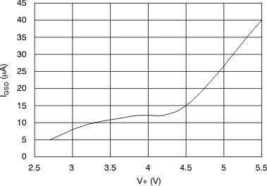
| IQSD | Quiescent current, shutdown mode | V+ = 5.5 V | 100 | µA | ||
| V+ = 3.8 V | 25 | |||||
| TEMPERATURE | ||||||
| TA | Specified range | -40 | 125 | °C | ||
6.6 Timing Requirements
At TA –40°C to +125°C and VS = 3V to 5.5V, unless otherwise noted.| FAST MODE(1) | HIGH-SPEED MODE(1) | UNIT | ||||
|---|---|---|---|---|---|---|
| MIN | MAX | MIN | MAX | |||
| f(SCL) | SCL operating frequency | 10 | 400 | 10 | 3400 | kHz |
| t(BUF) | Bus free time between STOP and START conditions | 600 | 160 | ns | ||
| t(HDSTA) | Hold time after repeated START condition. After this period, the first clock is generated. | 600 | 160 | ns | ||
| t(SUSTA) | Repeated START condition setup time | 600 | 160 | ns | ||
| t(SUSTO) | STOP condition setup time | 600 | 160 | ns | ||
| t(HDDAT) | Data hold time | 0(2) | 0(3) | ns | ||
| t(SUDAT) | Data setup time | 100 | 10 | ns | ||
| t(LOW) | Clock low period | 1300 | 160 | ns | ||
| t(HIGH) | Clock high period | 600 | 60 | ns | ||
| tR | Clock/Data input rise time | 300 | 160 | ns | ||
| tF | Clock/Data input fall time | 300 | 160 | ns | ||
 Figure 1. Serial Bus Interface Timing
6.7 Typical Characteristics
At TA = +25°C and V+ = 3 V to 5.5 V, unless otherwise noted.