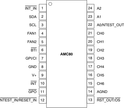
| 1 |
INT_IN |
Input |
Digital |
Interrupt input pin. An active low input that extends the INT_IN signal to the INT output of the AMC80. |
| 2 |
SDA |
I/O |
Digital |
Serial bus data line for SMBus, open-drain; requires pull-up resistor. |
| 3 |
SCL |
I/O |
Digital |
Serial bus clock line for SMBus, open-drain; requires pull-up resistor. |
| 4 |
FAN1 |
Input |
Digital |
Fan tachometer input pin |
| 5 |
FAN2 |
Input |
Digital |
Fan tachometer input pin |
| 6 |
BTI |
Input |
Digital |
Board temperature interrupt pin. BTI is driven by the over-temperature shutdown (OS) outputs of the additional temperature sensors. This pin has an internal 10-kΩ pull-up resistor. |
| 7 |
GPI(CI) |
Input |
Digital |
General-purpose input pin (chassis interrupt). An active high interrupt input pin to latch a chassis interrupt event. |
| 8 |
DGND |
Power |
Analog |
Digital ground. |
| 9 |
V+ |
Power |
Analog |
Positive supply voltage (3V to 5.5V). |
| 10 |
INT |
Output |
Digital |
Non-maskable interrupt (active high, PMOS, push-pull) or interrupt request (active low, NMOS, push-pull) pin. The INT pin becomes active when INT_IN, BTI, or GPI interrupts. This pin does not require a pullup resistor to V+. |
| 11 |
GPO |
Output |
Digital |
General-purpose output pin. GPO is an active low, NMOS, open-drain output. This pin is intended to drive an external power PMOS for software power control or to control power to a cooling fan. |
| 12 |
NTEST_IN/RESET_IN |
Input |
Digital |
This pin is an active-low input that enables NAND tree board-level connectivity testing. The AMC80 resets to its power-on state when NAND tree connectivity is enabled. |
| 13 |
RST_OUT/OS |
Output |
Digital |
This pin is an NMOS open-drain output. RST_OUT provides a master reset to devices connected to this line. OS is dedicated to the temperature reading alarm. |
| 14 |
AGND |
Power |
Analog |
Analog ground. This pin must be tied to a low-noise analog ground plane for optimum performance. |
| 15 |
CH6 |
Input |
Analog |
Analog input channel 6 |
| 16 |
CH5 |
Input |
Analog |
Analog input channel 5 |
| 17 |
CH4 |
Input |
Analog |
Analog input channel 4 |
| 18 |
CH3 |
Input |
Analog |
Analog input channel 3 |
| 19 |
CH2 |
Input |
Analog |
Analog input channel 2 |
| 20 |
CH1 |
Input |
Analog |
Analog input channel 1 |
| 21 |
CH0 |
Input |
Analog |
Analog input channel 0 |
| 22 |
A0/NTEST_OUT |
I/O |
Digital |
The lowest order bit of the serial bus address. During a NAND tree test for ATE board-level connectivity, this pin functions as an output. |
| 23 |
A1 |
Input |
Digital |
Address pin 1 |
| 24 |
A2 |
Input |
Digital |
Address pin 2 |
