SBOS559B May 2011 – October 2015 AMC80
PRODUCTION DATA.
- 1 Features
- 2 Applications
- 3 Description
- 4 Revision History
- 5 Pin Configuration and Functions
- 6 Specifications
-
7 Detailed Description
- 7.1 Overview
- 7.2 Functional Block Diagram
- 7.3 Feature Description
- 7.4 Programming
- 7.5
Register Map
- 7.5.1 Configuration Register
- 7.5.2 Interrupt Status Registers
- 7.5.3 Interrupt Mask Registers
- 7.5.4 Fan Divisor/RST_OUT/OS Register
- 7.5.5 OS Configuration/Temperature Resolution Register
- 7.5.6 Conversion Rate Register
- 7.5.7 Voltage/Temperature Channel Disable Register
- 7.5.8 Input Mode Register
- 7.5.9 ADC Control Register
- 7.5.10 Conversion Rate Count Register
- 7.5.11 Value Ram Register
- 8 Application and Implementation
- 9 Device and Documentation Support
- 10Mechanical, Packaging, and Orderable Information
Package Options
Mechanical Data (Package|Pins)
- PW|24
Thermal pad, mechanical data (Package|Pins)
Orderable Information
6 Specifications
6.1 Absolute Maximum Ratings(1)
Over operating free-air temperature range, unless otherwise noted.(1) Stresses above these ratings my cause permanent damage. Exposure to absolute maximum conditions for extended periods may degrade device reliability. These are stress ratings only, and functional operation of the device at these or any other conditions beyond those specified is not implied.
6.2 ESD Ratings
| VALUE | UNIT | |||
|---|---|---|---|---|
| V(ESD) | Electrostatic discharge | Human-body model (HBM), per ANSI/ESDA/JEDEC JS-001(1) | ±2500 | V |
| Charged-device model (CDM), per JEDEC specification JESD22-C101(2) | ±1000 | |||
| Machine model (MM) | ±200 | |||
(1) JEDEC document JEP155 states that 500-V HBM allows safe manufacturing with a standard ESD control process.
(2) JEDEC document JEP157 states that 250-V CDM allows safe manufacturing with a standard ESD control process. ance.
6.3 Recommended Operating Conditions
| MIN | NOM | MAX | UNIT | ||
|---|---|---|---|---|---|
| Supply voltage range, V+ | 3 | 5.5 | V | ||
| Input voltage range, VIN | –0.05 | (V+) + 0.05 | V | ||
| Operating temperature range, TA | –40 | 125 | °C | ||
6.4 Thermal Information
| THERMAL METRIC(1) | AMC80 | UNIT | |
|---|---|---|---|
| PW (TSSOP) | |||
| 24 PINS | |||
| RθJA | Junction-to-ambient thermal resistance | 100.72 | °C/W |
| RθJC(top) | Junction-to-case (top) thermal resistance | 31.4 | °C/W |
| RθJB | Junction-to-board thermal resistance | 54.7 | °C/W |
| ψJT | Junction-to-top characterization parameter | 1.0 | °C/W |
| ψJB | Junction-to-board characterization parameter | 54.2 | °C/W |
| RθJC(bot) | Junction-to-case (bottom) thermal resistance | N/A | °C/W |
(1) For more information about traditional and new thermal metrics, see the Semiconductor and IC Package Thermal Metrics application report, SPRA953.
6.5 Electrical Characteristics
At TA –40°C to +125°C and V+ = 3 V to 5.5 V, unless otherwise noted.| PARAMETER | TEST CONDITIONS | MIN | TYP | MAX | UNIT | |
|---|---|---|---|---|---|---|
| DIGITAL INPUTS | ||||||
| VIH | Input high voltage | 2 | V | |||
| VIL | Input low voltage | 0.8 | V | |||
| VHYS | Hysteresis voltage | V+ = 3.3 V | 0.23 | V | ||
| V+ = 5 V | 0.33 | V | ||||
| IIH | Input high current | VIH = V+, all pins except BTI | –1 | –0.005 | µA | |
| VIH = V+, BTI pin | –10 | –1 | µA | |||
| IIL | Input low current | VIL = 0 V, all pins except BTI | 0.005 | 1 | µA | |
| VIL = 0 V, V+ = 5.5 V, BTI pin | 2 | mA | ||||
| CIN | Input capacitance | 20 | pF | |||
| ANALOG INPUTS | ||||||
| VIN | Input voltage range | Default | 0 | 2.56 | V | |
| Programmable | 0 | V+ | V | |||
| IL-ON | Input leakage current (on) | ±0.005 | µA | |||
| IL-OFF | Input leakage current (off) | ±0.005 | µA | |||
| RIN | Input resistance | 2 | 10 | kΩ | ||
| DIGITAL OUTPUTS (A0/NTEST_OUT, INT) | ||||||
| VOH | Output high voltage | IOUT = 3 mA/5 mA, V+ = 3 V/4.5 V | 2.4 | V | ||
| VOL | Output low voltage | IOUT = 3 mA/5 mA, V+ = 3 V/4.5 V | 0.4 | V | ||
| DIGITAL OPEN-DRAIN OUTPUTS (GPO, RST_OUT/OS, GPI/CI, SDA) | ||||||
| VOL | Output low voltage | IOUT = 3 mA/5 mA, V+ = 3 V/4.5 V, all pins except SDA |
0.4 | V | ||
| IOUT = 4 mA, V+ = 3 V, SDA pin | 0.4 | |||||
| IOH | Output high current | VOUT = V+ | 0.005 | 1 | µA | |
| tw | Pulse duration | RST_OUT/OS, GPI/CI | 10 | 22.5 | ms | |
| SMBus | ||||||
| SMBus timeout(1) | 28 | 35 | ms | |||
| TEMPERATURE ERROR | ||||||
| TE | Temperature error | TA = –40°C to +125°C | ±3 | °C | ||
| TA = –25°C to +100°C | ±2 | °C | ||||
| TR | Temperature resolution | 0.0625 | °C | |||
| ANALOG-TO-DIGITAL CONVERTER | ||||||
| VR | Resolution | VIN = 2.56 V | 2.5 | mV | ||
| VIN = V+ | 6 | |||||
| DNL | Differential linearity | –1 | 1 | LSB(2) | ||
| ADCERR | Total unadjusted error(3) | –1% | 1% | |||
| PSRR | Power supply rejection ratio | ±0.0008% | ||||
| tC(4) | Total conversion time | 662 | 728 | 810 | ms | |
| FAN RPM-TO-DIGITAL CONVERTER | ||||||
| FANERR | Fan RPM error | –10% | 10% | |||
| fCLK | Internal clock frequency | 20.2 | 22.5 | 24.8 | kHz | |
| FANRPM | FAN1 and FAN2 nominal input RPM | Divisor = 1, fan count = 153 | 8800 | RPM | ||
| Divisor = 2, fan count = 153 | 4400 | |||||
| Divisor = 3, fan count = 153 | 2200 | |||||
| Divisor = 4, fan count = 153 | 1100 | |||||
| FSC | Full-scale count | 255 | Counts | |||
| POWER SUPPLY | ||||||
| V+ | Specified voltage range | 3 | 5.5 | V | ||
| IQA | Quiescent current, average | V+ = 5.5 V | 100 | µA | ||
| V+ = 3.8 V | 25 | |||||
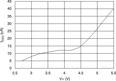
| IQSD | Quiescent current, shutdown mode | V+ = 5.5 V | 100 | µA | ||
| V+ = 3.8 V | 25 | |||||
| TEMPERATURE | ||||||
| TA | Specified range | -40 | 125 | °C | ||
(1) The SMBus timeout in the AMC80 resets the interface anytime SCL or SDA is low for over 28 ms.
(2) LSB means least significant bit.
(3) Total unadjusted error contains offset, gain, and linearity errors of the ADC.
(4) Total conversion time contains the temperature conversion, the seven analog input voltage conversions, and the two tachometer readings.
6.6 Timing Requirements
At TA –40°C to +125°C and VS = 3V to 5.5V, unless otherwise noted.| FAST MODE(1) | HIGH-SPEED MODE(1) | UNIT | ||||
|---|---|---|---|---|---|---|
| MIN | MAX | MIN | MAX | |||
| f(SCL) | SCL operating frequency | 10 | 400 | 10 | 3400 | kHz |
| t(BUF) | Bus free time between STOP and START conditions | 600 | 160 | ns | ||
| t(HDSTA) | Hold time after repeated START condition. After this period, the first clock is generated. | 600 | 160 | ns | ||
| t(SUSTA) | Repeated START condition setup time | 600 | 160 | ns | ||
| t(SUSTO) | STOP condition setup time | 600 | 160 | ns | ||
| t(HDDAT) | Data hold time | 0(2) | 0(3) | ns | ||
| t(SUDAT) | Data setup time | 100 | 10 | ns | ||
| t(LOW) | Clock low period | 1300 | 160 | ns | ||
| t(HIGH) | Clock high period | 600 | 60 | ns | ||
| tR | Clock/Data input rise time | 300 | 160 | ns | ||
| tF | Clock/Data input fall time | 300 | 160 | ns | ||
(1) Values based on a statistical analysis of a one-time sample of devices. Minimum and maximum values are not specified and not production tested.
(2) For cases when the fall time of SCL is less than 20 ns and/or the rise time or fall time of SDA is less than 20 ns, the hold time should be greater than 20 ns.
(3) For cases when the fall time of SCL is less than 10 ns and/or the rise or fall time of SDA is less than 10 ns, the hold time should be greater than 10 ns.
 Figure 1. Serial Bus Interface Timing
6.7 Typical Characteristics
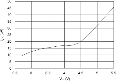
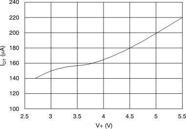
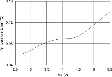
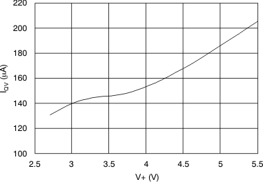
At TA = +25°C and V+ = 3 V to 5.5 V, unless otherwise noted.