SWRS203D May   2017  – September 2024 AWR1642

PRODUCTION DATA  

  1.   1
  2. Features
  3. Applications
  4. Description
  5. Functional Block Diagram
  6. Device Comparison
    1. 5.1 Related Products
  7. Terminal Configuration and Functions
    1. 6.1 Pin Diagram
    2. 6.2 Signal Descriptions
      1. 6.2.1 Signal Descriptions - Digital
      2. 6.2.2 Signal Descriptions - Analog
    3. 6.3 Pin Attributes
  8. Specifications
    1. 7.1  Absolute Maximum Ratings
    2. 7.2  ESD Ratings
    3. 7.3  Power-On Hours (POH)
    4. 7.4  Recommended Operating Conditions
    5. 7.5  Power Supply Specifications
    6. 7.6  Power Consumption Summary
    7. 7.7  RF Specification
    8. 7.8  CPU Specifications
    9. 7.9  Thermal Resistance Characteristics for FCBGA Package [ABL0161]
    10. 7.10 Timing and Switching Characteristics
      1. 7.10.1  Power Supply Sequencing and Reset Timing
      2. 7.10.2  Input Clocks and Oscillators
        1. 7.10.2.1 Clock Specifications
      3. 7.10.3  Multibuffered / Standard Serial Peripheral Interface (MibSPI)
        1. 7.10.3.1 Peripheral Description
        2. 7.10.3.2 MibSPI Transmit and Receive RAM Organization
          1. 7.10.3.2.1 SPI Timing Conditions
          2. 7.10.3.2.2 SPI Controller Mode Switching Parameters (CLOCK PHASE = 0, SPICLK = output, SPISIMO = output, and SPISOMI = input) #GUID-C70CFB1F-161A-495B-85B8-62E1C643D037/T4362547-236 #GUID-C70CFB1F-161A-495B-85B8-62E1C643D037/T4362547-237 #GUID-C70CFB1F-161A-495B-85B8-62E1C643D037/T4362547-238
          3. 7.10.3.2.3 SPI Controller Mode Switching Parameters (CLOCK PHASE = 1, SPICLK = output, SPISIMO = output, and SPISOMI = input) #GUID-F724BCC6-8F26-42C4-8723-451EDE9A36D3/T4362547-244 #GUID-F724BCC6-8F26-42C4-8723-451EDE9A36D3/T4362547-245 #GUID-F724BCC6-8F26-42C4-8723-451EDE9A36D3/T4362547-246
        3. 7.10.3.3 SPI Peripheral Mode I/O Timings
          1. 7.10.3.3.1 SPI Peripheral Mode Switching Parameters (SPICLK = input, SPISIMO = input, and SPISOMI = output) #GUID-1B5DE4C6-14B2-48EF-965D-3B03E1AE325B/T4362547-70 #GUID-1B5DE4C6-14B2-48EF-965D-3B03E1AE325B/T4362547-71 #GUID-1B5DE4C6-14B2-48EF-965D-3B03E1AE325B/T4362547-73
        4. 7.10.3.4 Typical Interface Protocol Diagram (Peripheral Mode)
      4. 7.10.4  LVDS Interface Configuration
        1. 7.10.4.1 LVDS Interface Timings
      5. 7.10.5  General-Purpose Input/Output
        1. 7.10.5.1 Switching Characteristics for Output Timing versus Load Capacitance (CL)
      6. 7.10.6  Controller Area Network Interface (DCAN)
        1. 7.10.6.1 Dynamic Characteristics for the DCANx TX and RX Pins
      7. 7.10.7  Controller Area Network - Flexible Data-rate (CAN-FD)
        1. 7.10.7.1 Dynamic Characteristics for the CANx TX and RX Pins
      8. 7.10.8  Serial Communication Interface (SCI)
        1. 7.10.8.1 SCI Timing Requirements
      9. 7.10.9  Inter-Integrated Circuit Interface (I2C)
        1. 7.10.9.1 I2C Timing Requirements #GUID-36963FBF-DA1A-4FF8-B71D-4A185830E708/T4362547-185
      10. 7.10.10 Quad Serial Peripheral Interface (QSPI)
        1. 7.10.10.1 QSPI Timing Conditions
        2. 7.10.10.2 Timing Requirements for QSPI Input (Read) Timings #GUID-6DC69BBB-F187-4499-AC42-8C006552DEE1/T4362547-210 #GUID-6DC69BBB-F187-4499-AC42-8C006552DEE1/T4362547-209
        3. 7.10.10.3 QSPI Switching Characteristics
      11. 7.10.11 ETM Trace Interface
        1. 7.10.11.1 ETMTRACE Timing Conditions
        2. 7.10.11.2 ETM TRACE Switching Characteristics
      12. 7.10.12 Data Modification Module (DMM)
        1. 7.10.12.1 DMM Timing Requirements
      13. 7.10.13 JTAG Interface
        1. 7.10.13.1 JTAG Timing Conditions
        2. 7.10.13.2 Timing Requirements for IEEE 1149.1 JTAG
        3. 7.10.13.3 Switching Characteristics Over Recommended Operating Conditions for IEEE 1149.1 JTAG
  9. Detailed Description
    1. 8.1 Overview
    2. 8.2 Functional Block Diagram
    3. 8.3 Subsystems
      1. 8.3.1 RF and Analog Subsystem
        1. 8.3.1.1 Clock Subsystem
        2. 8.3.1.2 Transmit Subsystem
        3. 8.3.1.3 Receive Subsystem
      2. 8.3.2 Processor Subsystem
      3. 8.3.3 Automotive Interface
      4. 8.3.4 Main Subsystem Cortex-R4F Memory Map
      5. 8.3.5 DSP Subsystem Memory Map
    4. 8.4 Other Subsystems
      1. 8.4.1 ADC Channels (Service) for User Application
        1. 8.4.1.1 GP-ADC Parameter
  10. Monitoring and Diagnostics
    1. 9.1 Monitoring and Diagnostic Mechanisms
      1. 9.1.1 Error Signaling Module
  11. 10Applications, Implementation, and Layout
    1. 10.1 Application Information
    2. 10.2 Short-Range Radar
    3. 10.3 Reference Schematic
  12. 11Device and Documentation Support
    1. 11.1 Device Nomenclature
    2. 11.2 Tools and Software
    3. 11.3 Documentation Support
    4. 11.4 Support Resources
    5. 11.5 Trademarks
    6. 11.6 Electrostatic Discharge Caution
    7. 11.7 Glossary
  13. 12Revision History
  14. 13Mechanical, Packaging, and Orderable Information
    1. 13.1 Packaging Information
    2. 13.2 Tray Information for

Package Options

Mechanical Data (Package|Pins)
Thermal pad, mechanical data (Package|Pins)
Orderable Information

Packaging Information

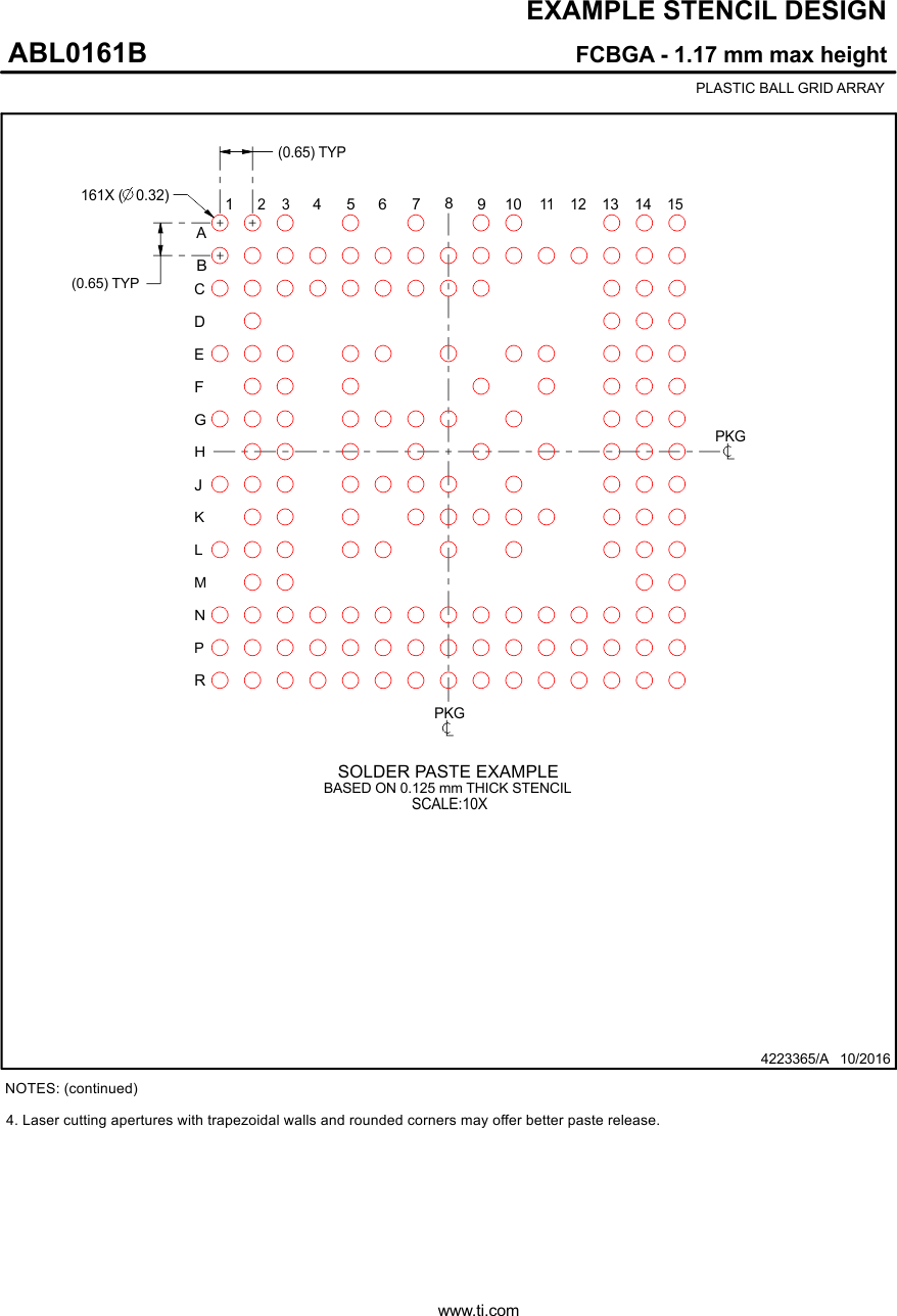
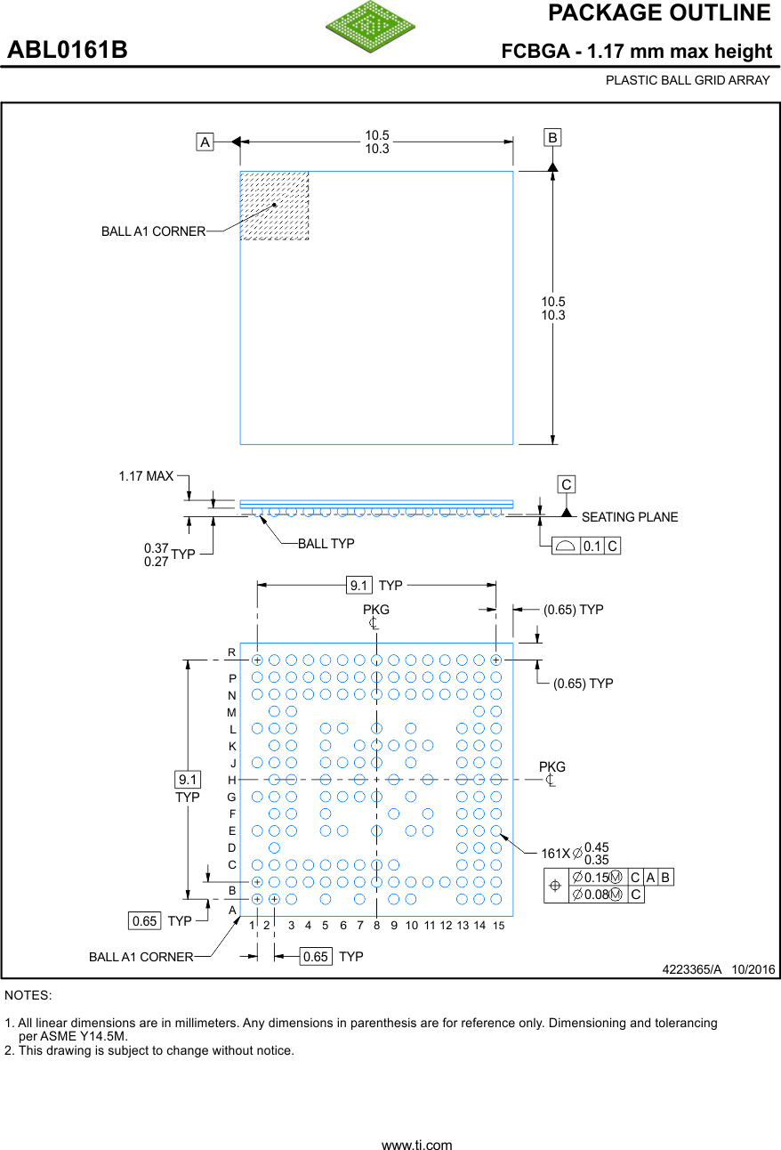
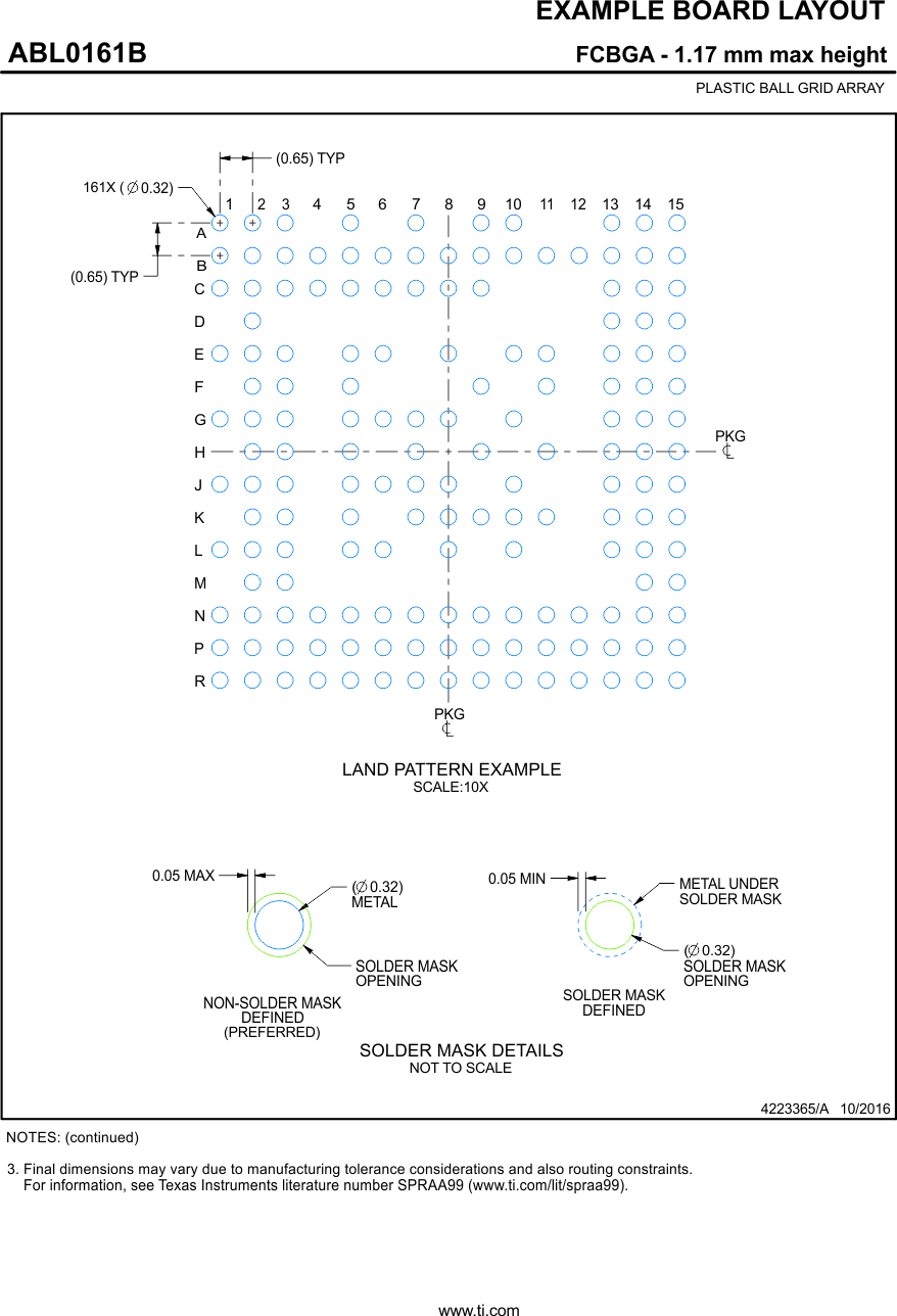
The following pages include mechanical, packaging, and orderable information. This information is the most current data available for the designated devices. This data is subject to change without notice and revision of this document. For browser-based versions of this data sheet, refer to the left-hand navigation.
AWR1642
AWR1642
AWR1642