SWRS314A January 2024 – November 2024 AWR2544
ADVANCE INFORMATION
- 1
- 1 Features
- 2 Applications
- 3 Description
- 4 Device Comparison
- 5 Related Products
- 6 Pin Configurations and Functions
-
7 Specifications
- 7.1 Absolute Maximum Ratings
- 7.2 ESD Ratings
- 7.3 Power-On Hours (POH)
- 7.4 Recommended Operating Conditions
- 7.5 VPP Specifications for One-Time Programmable (OTP) eFuses
- 7.6 Power Supply Specifications
- 7.7 Power Consumption Summary
- 7.8 RF Specifications
- 7.9 Thermal Resistance Characteristics
- 7.10 Power Supply Sequencing and Reset Timing
- 7.11 Input Clocks and Oscillators
- 7.12
Peripheral Information
- 7.12.1
QSPI Flash Memory Peripheral
- 7.12.1.1 QSPI Timing Conditions
- 7.12.1.2 QSPI Timing Requirements #GUID-C38B9713-DC57-4B3B-8AFF-A79AF70E5A5A/GUID-97D19708-D87E-443B-9ADF-1760CFEF6F4C #GUID-C38B9713-DC57-4B3B-8AFF-A79AF70E5A5A/GUID-0A61EEC9-2B95-4C27-B219-18D27C8F9430
- 7.12.1.3 QSPI Switching Characteristics #GUID-D1480E86-4079-4A44-A68A-26C2D9F4506B/T4362547-64 #GUID-D1480E86-4079-4A44-A68A-26C2D9F4506B/T4362547-65
- 7.12.2
Multibuffered / Standard Serial Peripheral Interface (MibSPI)
- 7.12.2.1 MibSPI Peripheral Description
- 7.12.2.2
MibSPI Transmit and Receive RAM Organization
- 7.12.2.2.1 SPI Timing Conditions
- 7.12.2.2.2 SPI Controller Mode Switching Parameters (CLOCK PHASE = 0, SPICLK = output, SPISIMO = output, and SPISOMI = input) #GUID-3DD8619F-41DB-47CF-9AF7-5916CFF97E61/T4362547-236 #GUID-3DD8619F-41DB-47CF-9AF7-5916CFF97E61/T4362547-237 #GUID-3DD8619F-41DB-47CF-9AF7-5916CFF97E61/T4362547-238
- 7.12.2.2.3 SPI Controller Mode Switching Parameters (CLOCK PHASE = 1, SPICLK = output, SPISIMO = output, and SPISOMI = input) #GUID-220CE6B8-D17E-48AF-BF69-AAEC97D55C95/T4362547-244 #GUID-220CE6B8-D17E-48AF-BF69-AAEC97D55C95/T4362547-245 #GUID-220CE6B8-D17E-48AF-BF69-AAEC97D55C95/T4362547-246
- 7.12.2.3 SPI Peripheral Mode I/O Timings
- 7.12.3
Ethernet Switch (RGMII/RMII/MII)
Peripheral
- 7.12.3.1 RGMII/RMII/MII Timing Conditions
- 7.12.3.2 RGMII Transmit Clock Switching Characteristics
- 7.12.3.3 RGMII Transmit Data and Control Switching Characteristics
- 7.12.3.4 RGMII Receive Clock Timing Requirements
- 7.12.3.5 RGMII Receive Data and Control Timing Requirements
- 7.12.3.6 RMII Transmit Clock Switching Characteristics
- 7.12.3.7 RMII Transmit Data and Control Switching Characteristics
- 7.12.3.8 RMII Receive Clock Timing Requirements
- 7.12.3.9 RMII Receive Data and Control Timing Requirements
- 7.12.3.10 MII Transmit Switching Characteristics
- 7.12.3.11 MII Receive Clock Timing Requirements
- 7.12.3.12 MII Receive Timing Requirements
- 7.12.3.13 MII Transmit Clock Timing Requirements
- 7.12.3.14 MDIO Interface Timings
- 7.12.4 LVDS Instrumentation and Measurement Peripheral
- 7.12.5 UART Peripheral
- 7.12.6 Inter-Integrated Circuit Interface (I2C)
- 7.12.7 Enhanced Pulse-Width Modulator (ePWM)
- 7.12.8 General-Purpose Input/Output
- 7.12.1
QSPI Flash Memory Peripheral
- 7.13 Emulation and Debug
- 8 Detailed Description
- 9 Monitoring and Diagnostics
- 10Applications, Implementation, and Layout
- 11Device and Documentation Support
- 12Revision History
- 13Mechanical, Packaging, and Orderable Information
Package Options
Mechanical Data (Package|Pins)
- AMQ|248
Thermal pad, mechanical data (Package|Pins)
Orderable Information
7.8 RF Specifications
over recommended operating conditions and with run time calibrations enabled
(unless otherwise noted)
| PARAMETER | MIN | TYP | MAX | UNIT | ||
|---|---|---|---|---|---|---|
| Receiver | Noise figure | 13 | dB | |||
| 1-dB compression point (Out Of Band)(1) | -8 | dBm | ||||
| Maximum gain | 44 | dB | ||||
| Gain range | 20 | dB | ||||
| Gain step size | 2 | dB | ||||
| IF bandwidth(2) | 20 | MHz | ||||
| ADC sampling rate |
45 |
Msps | ||||
| ADC resolution | 12 | Bits | ||||
| Return loss (S11) | -8 | dB | ||||
| Gain mismatch variation (over temperature) | ±0.5 | dB | ||||
| Phase mismatch variation (over temperature) | ±3 | ° | ||||
| Idle Channel Spurs | -90 | dBFS | ||||
| Transmitter | Output power |
+12 |
dBm |
|||
| Phase shifter accuracy | ±5 | ° | ||||
| Temperature sensor accuracy | ±5 | ℃ | ||||
| Amplitude noise | -145 | dBc/Hz | ||||
| Clock subsystem | Frequency range | 76 | 81 | GHz | ||
| Ramp rate | 250(3) | MHz/μs | ||||
| Phase noise at 1-MHz offset | 76 to 77 GHz (VCO1) | -96 | dBc/Hz | |||
| 76 to 81 GHz (VCO2)(4) | -95 | |||||
(1) 1-dB Compression Point (Out Of
Band) is measured by feeding a continuous wave tone at 5% of the programmed HPF
cut-off frequency (i.e. blocker tone). The compression point is determined by
the blocker power that results in a 1dB compression of the blocker tone at the
RX ADC.
(2) The analog IF stages include a second order high pass filter that can
be configured to the following -6dB corner frequencies:
The filtering performed by the digital baseband chain is targeted to
provide:
| Available HPF Corner Frequencies (kHz) |
| HPF |
| 300, 350, 700, 1400, |
- Less than ±0.5 dB pass-band ripple/droop, and
- Better than 60 dB anti-aliasing attenuation for any frequency that can alias back into the pass-band.
(3) The max ramp rate depends on the PLL bandwidth configuration
set using the"AWR_APLL_SYNTH_BW_CONTROL_SB" API. For more details, refer to the
mmWave Radar Interface Control document.
(4) VCO2 supports a maximum
continuous range of 4.5GHz. The supported range can span 76-80.5GHz or
76.5-81GHz through VCO2_RANGE_CONFIG in AWR_ CAL_MON_FREQUENCY_* API.
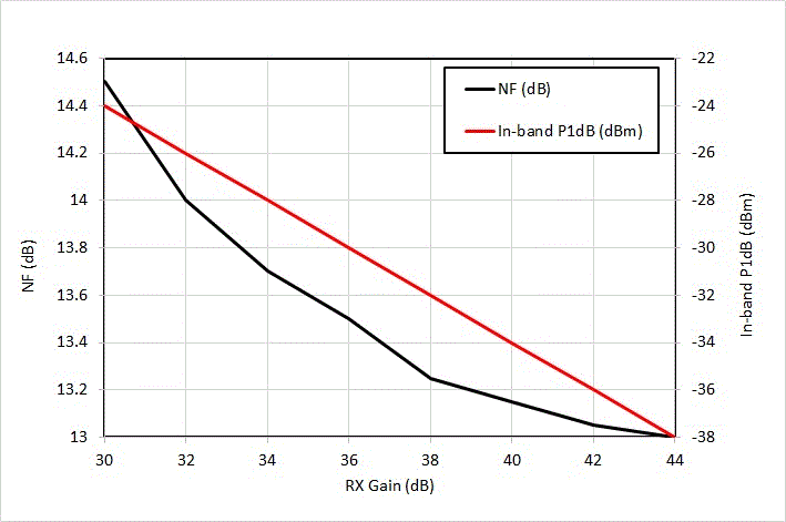
Figure 7-1 shows variations of noise figure and in-band P1dB parameters with respect to receiver gain programmed
 Figure 7-1 Noise Figure, In-band P1dB vs
Receiver Gain