SWRS273D November 2021 – September 2024 AWR2944
PRODUCTION DATA
- 1
- 1 Features
- 2 Applications
- 3 Description
- 4 Device Comparison
- 5 Pin Configurations and Functions
-
6 Specifications
- 6.1 Absolute Maximum Ratings
- 6.2 ESD Ratings
- 6.3 Power-On Hours (POH)
- 6.4 Recommended Operating Conditions
- 6.5 VPP Specifications for One-Time Programmable (OTP) eFuses
- 6.6 Power Supply Specifications
- 6.7 Power Consumption Summary
- 6.8 RF Specifications
- 6.9 Thermal Resistance Characteristics
- 6.10 Power Supply Sequencing and Reset Timing
- 6.11 Input Clocks and Oscillators
- 6.12
Peripheral Information
- 6.12.1
QSPI Flash Memory Peripheral
- 6.12.1.1 QSPI Timing Conditions
- 6.12.1.2 QSPI Timing Requirements #GUID-CD30070D-F132-4A2C-92CD-5AA96AE70B94/GUID-97D19708-D87E-443B-9ADF-1760CFEF6F4C #GUID-CD30070D-F132-4A2C-92CD-5AA96AE70B94/GUID-0A61EEC9-2B95-4C27-B219-18D27C8F9430
- 6.12.1.3 QSPI Switching Characteristics #GUID-20B35D26-AFE6-451C-B9E9-B3F2FA08097C/T4362547-64 #GUID-20B35D26-AFE6-451C-B9E9-B3F2FA08097C/T4362547-65
- 6.12.2
Multibuffered / Standard Serial Peripheral Interface (MibSPI)
- 6.12.2.1 MibSPI Peripheral Description
- 6.12.2.2
MibSPI Transmit and Receive RAM Organization
- 6.12.2.2.1 SPI Timing Conditions
- 6.12.2.2.2 SPI Controller Mode Switching Parameters (CLOCK PHASE = 0, SPICLK = output, SPISIMO = output, and SPISOMI = input) #GUID-20BA2ACF-4FC2-43F6-960F-1A4CA56E65A6/T4362547-236 #GUID-20BA2ACF-4FC2-43F6-960F-1A4CA56E65A6/T4362547-237 #GUID-20BA2ACF-4FC2-43F6-960F-1A4CA56E65A6/T4362547-238
- 6.12.2.2.3 SPI Controller Mode Switching Parameters (CLOCK PHASE = 1, SPICLK = output, SPISIMO = output, and SPISOMI = input) #GUID-517E5284-3345-461F-B07F-EB95741B1272/T4362547-244 #GUID-517E5284-3345-461F-B07F-EB95741B1272/T4362547-245 #GUID-517E5284-3345-461F-B07F-EB95741B1272/T4362547-246
- 6.12.2.3 SPI Peripheral Mode I/O Timings
- 6.12.3
Ethernet Switch (RGMII/RMII/MII)
Peripheral
- 6.12.3.1 RGMII Timing Conditions
- 6.12.3.2 RGMII Transmit Clock Switching Characteristics
- 6.12.3.3 RGMII Transmit Data and Control Switching Characteristics
- 6.12.3.4 RGMII Receive Clock Timing Requirements
- 6.12.3.5 RGMII Receive Data and Control Timing Requirements
- 6.12.3.6 RMII Transmit Clock Switching Characteristics
- 6.12.3.7 RMII Transmit Data and Control Switching Characteristics
- 6.12.3.8 RMII Receive Clock Timing Requirements
- 6.12.3.9 RMII Receive Data and Control Timing Requirements
- 6.12.3.10 MII Transmit Switching Characteristics
- 6.12.3.11 MII Receive Clock Timing Requirements
- 6.12.3.12 MII Receive Timing Requirements
- 6.12.3.13 MII Transmit Clock Timing Requirements
- 6.12.3.14 MDIO Interface Timings
- 6.12.4 LVDS/Aurora Instrumentation and Measurement Peripheral
- 6.12.5 UART Peripheral
- 6.12.6 Inter-Integrated Circuit Interface (I2C)
- 6.12.7 Controller Area Network - Flexible Data-rate (CAN-FD)
- 6.12.8 CSI2 Receiver Peripheral
- 6.12.9 Enhanced Pulse-Width Modulator (ePWM)
- 6.12.10 General-Purpose Input/Output
- 6.12.1
QSPI Flash Memory Peripheral
- 6.13 Emulation and Debug
- 7 Detailed Description
- 8 Monitoring and Diagnostics
- 9 Applications, Implementation, and Layout
- 10Device and Documentation Support
- 11Revision History
- 12Mechanical, Packaging, and Orderable Information
Package Options
Mechanical Data (Package|Pins)
- ALT|266
Thermal pad, mechanical data (Package|Pins)
Orderable Information
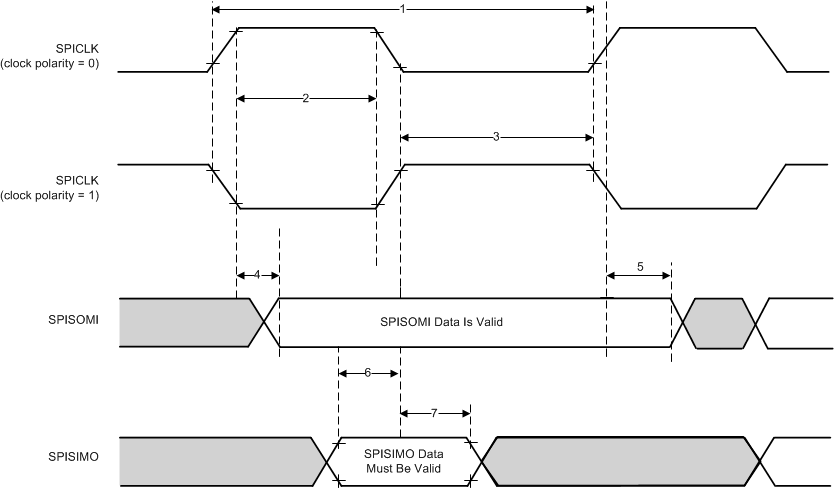
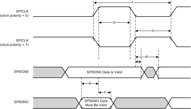
6.12.2.3.1 SPI Peripheral Mode Switching Parameters (SPICLK = input, SPISIMO = input,
and SPISOMI = output)(1)(2)(3)
| SPECIFICATION NUMBER | PARAMETER(5) | MIN | TYP | MAX | UNIT | |
|---|---|---|---|---|---|---|
| 1 | tc(SPC)S | Cycle time, SPICLK (4) | 20 | ns | ||
| 2 | tw(SPCH)S | Pulse duration, SPICLK high (clock polarity = 0) | 8 | ns | ||
| tw(SPCL)S | Pulse duration, SPICLK low (clock polarity = 1) | 8 | ||||
| 3 | tw(SPCL)S | Pulse duration, SPICLK low (clock polarity = 0) | 8 | ns | ||
| tw(SPCH)S | Pulse duration, SPICLK high (clock polarity = 1) | 8 | ||||
| 4 | td(SPCH-SOMI)S | Delay time, SPISOMI valid after SPICLK high (clock polarity = 0) | 10 | ns | ||
| td(SPCL-SOMI)S | Delay time, SPISOMI valid after SPICLK low (clock polarity = 1) | 10 | ||||
| 5 | th(SPCH-SOMI)S | Hold time, SPISOMI data valid after SPICLK high (clock polarity = 0) | 2 | ns | ||
| th(SPCL-SOMI)S | Hold time, SPISOMI data valid after SPICLK low (clock polarity = 1) | 2 | ||||
| 4 | td(SPCH-SOMI)S | Delay time, SPISOMI valid after SPICLK high (clock polarity = 0; clock phase = 0) OR (clock polarity = 1; clock phase = 1) | 14 | ns | ||
| td(SPCL-SOMI)S | Delay time, SPISOMI valid after SPICLK low (clock polarity = 1; clock phase = 0) OR (clock polarity = 0; clock phase = 1) | 14 | ||||
| 5 | th(SPCH-SOMI)S | Hold time, SPISOMI data valid after SPICLK high (clock polarity = 0; clock phase = 0) OR (clock polarity = 1; clock phase = 1) | 2 | ns | ||
| th(SPCL-SOMI)S | Hold time, SPISOMI data valid after SPICLK low (clock polarity = 1; clock phase = 0) OR (clock polarity = 0; clock phase = 1) | 2 | ||||
| 6 | tsu(SIMO-SPCL)S | Setup time, SPISIMO before SPICLK low (clock polarity = 0; clock phase = 0) OR (clock polarity = 1; clock phase = 1) | 2.1 | ns | ||
| tsu(SIMO-SPCH)S | Setup time, SPISIMO before SPICLK high (clock polarity = 1; clock phase = 0) OR (clock polarity = 0; clock phase = 1) | 2.1 | ||||
| 7 | th(SPCL-SIMO)S | Hold time, SPISIMO data valid after SPICLK low (clock polarity = 0; clock phase = 0) OR (clock polarity = 1; clock phase = 1) | 1 | ns | ||
| th(SPCL-SIMO)S | Hold time, SPISIMO data valid after SPICLK high (clock polarity = 1; clock phase = 0) OR (clock polarity = 0; clock phase = 1) | 1 | ||||
(1) The Controller bit (SPIGCRx.0) is cleared ( where x = 0 or 1 ).
(2) The CLOCK PHASE bit (SPIFMTx.16) is either cleared or set for CLOCK PHASE = 0 or CLOCK PHASE = 1 respectively.
(3) tc(MSS_VCLK) = main subsystem clock time = 1 / f(MSS_VCLK). For more details, refer to the device Technical Reference Manual.
(4) When the SPI is in Peripheral mode, the following must be true: For PS values from 1 to 255: tc(SPC)S ≥ (PS +1)tc(MSS_VCLK) ≥ 25 ns, where PS is the prescale value set in the SPIFMTx.[15:8] register bits.For PS values of 0: tc(SPC)S = 2tc(MSS_VCLK) ≥ 25 ns.
(5) The active edge of the SPICLK signal referenced is controlled by the CLOCK POLARITY bit (SPIFMTx.17).
 Figure 6-10 SPI Peripheral Mode External Timing (CLOCK PHASE = 0)
 Figure 6-11 SPI Peripheral Mode External Timing (CLOCK PHASE = 1)