SWRS296B July   2023  – June 2024 AWRL1432

PRODUCTION DATA  

  1.   1
  2. Features
  3. Applications
  4. Description
  5. Functional Block Diagram
  6. Device Comparison
    1. 5.1 Related Products
  7. Terminal Configurations and Functions
    1. 6.1 Pin Diagrams
    2. 6.2 Signal Descriptions
      1.      11
      2.      12
      3.      13
      4.      14
      5.      15
      6.      16
      7.      17
      8.      18
      9.      19
      10.      20
      11.      21
      12.      22
      13.      23
      14.      24
      15.      25
      16.      26
      17.      27
    3.     28
  8. Specifications
    1. 7.1  Absolute Maximum Ratings
    2. 7.2  ESD Ratings
    3. 7.3  Power-On Hours (POH)
    4. 7.4  Recommended Operating Conditions
    5. 7.5  VPP Specifications for One-Time Programmable (OTP) eFuses
      1. 7.5.1 Recommended Operating Conditions for OTP eFuse Programming
      2. 7.5.2 Hardware Requirements
      3. 7.5.3 Impact to Your Hardware Warranty
    6. 7.6  Power Supply Specifications
      1. 7.6.1 Power Optimized 3.3V I/O Topology
      2. 7.6.2 BOM Optimized 3.3V I/O Topology
      3. 7.6.3 Power Optimized 1.8V I/O Topology
      4. 7.6.4 BOM Optimized 1.8V I/O Topology
      5. 7.6.5 System Topologies
        1. 7.6.5.1 Power Topologies
          1. 7.6.5.1.1 BOM Optimized Mode
          2. 7.6.5.1.2 Power Optimized Mode
      6. 7.6.6 Internal LDO output decoupling capacitor and layout conditions for BOM optimized topology
        1. 7.6.6.1 Single-capacitor rail
          1. 7.6.6.1.1 1.2V Digital LDO
        2. 7.6.6.2 Two-capacitor rail
          1. 7.6.6.2.1 1.2V RF LDO
          2. 7.6.6.2.2 1.2V SRAM LDO
          3. 7.6.6.2.3 1.0V RF LDO
      7. 7.6.7 Noise and Ripple Specifications
    7. 7.7  Power Save Modes
      1. 7.7.1 Typical Power Consumption Numbers
    8. 7.8  Peak Current Requirement per Voltage Rail
    9. 7.9  RF Specification
    10. 7.10 Supported Front End features
    11. 7.11 CPU Specifications
    12. 7.12 Thermal Resistance Characteristics
    13. 7.13 Timing and Switching Characteristics
      1. 7.13.1  Power Supply Sequencing and Reset Timing
      2. 7.13.2  Synchronized Frame Triggering
      3. 7.13.3  Input Clocks and Oscillators
        1. 7.13.3.1 Clock Specifications
      4. 7.13.4  MultiChannel buffered / Standard Serial Peripheral Interface (McSPI)
        1. 7.13.4.1 McSPI Features
        2. 7.13.4.2 SPI Timing Conditions
        3. 7.13.4.3 SPI—Controller Mode
          1. 7.13.4.3.1 Timing and Switching Requirements for SPI - Controller Mode
          2. 7.13.4.3.2 Timing and Switching Characteristics for SPI Output Timings—Controller Mode
        4. 7.13.4.4 SPI—Peripheral Mode
          1. 7.13.4.4.1 Timing and Switching Requirements for SPI - Peripheral Mode
          2. 7.13.4.4.2 Timing and Switching Characteristics for SPI Output Timings—Secondary Mode
      5. 7.13.5  RDIF Interface Configuration
        1. 7.13.5.1 RDIF Interface Timings
        2. 7.13.5.2 RDIF Data Format
      6. 7.13.6  LIN
      7. 7.13.7  General-Purpose Input/Output
        1. 7.13.7.1 Switching Characteristics for Output Timing versus Load Capacitance (CL)
      8. 7.13.8  Controller Area Network - Flexible Data-rate (CAN-FD)
        1. 7.13.8.1 Dynamic Characteristics for the CANx TX and RX Pins
      9. 7.13.9  Serial Communication Interface (SCI)
        1. 7.13.9.1 SCI Timing Requirements
      10. 7.13.10 Inter-Integrated Circuit Interface (I2C)
        1. 7.13.10.1 I2C Timing Requirements
      11. 7.13.11 Quad Serial Peripheral Interface (QSPI)
        1. 7.13.11.1 QSPI Timing Conditions
        2. 7.13.11.2 Timing Requirements for QSPI Input (Read) Timings
        3. 7.13.11.3 QSPI Switching Characteristics
      12. 7.13.12 JTAG Interface
        1. 7.13.12.1 JTAG Timing Conditions
        2. 7.13.12.2 Timing Requirements for IEEE 1149.1 JTAG
        3. 7.13.12.3 Switching Characteristics Over Recommended Operating Conditions for IEEE 1149.1 JTAG
  9. Detailed Description
    1. 8.1 Overview
    2. 8.2 Functional Block Diagram
    3. 8.3 Subsystems
      1. 8.3.1 RF and Analog Subsystem
      2. 8.3.2 Clock Subsystem
      3. 8.3.3 Transmit Subsystem
      4. 8.3.4 Receive Subsystem
      5. 8.3.5 Processor Subsystem
      6. 8.3.6 Automotive Interface
      7. 8.3.7 Host Interface
      8. 8.3.8 Application Subsystem
      9. 8.3.9 Hardware Accelerator (HWA1.2) Features
        1. 8.3.9.1 Hardware Accelerator Feature Differences Between HWA1.1 and HWA1.2
    4. 8.4 Other Subsystems
      1. 8.4.1 GPADC Channels (Service) for User Application
      2. 8.4.2 GPADC Parameters
    5. 8.5 Memory Partitioning Options
    6. 8.6 Boot Modes
  10. Monitoring and Diagnostics
  11. 10Applications, Implementation, and Layout
    1. 10.1 Application Information
    2. 10.2 Reference Schematic
  12. 11Device and Documentation Support
    1. 11.1 Device Nomenclature
    2. 11.2 Tools and Software
    3. 11.3 Documentation Support
    4. 11.4 Support Resources
    5. 11.5 Trademarks
    6. 11.6 Electrostatic Discharge Caution
    7. 11.7 Glossary
  13. 12Revision History
  14. 13Mechanical, Packaging, and Orderable Information

Package Options

Mechanical Data (Package|Pins)
  • AMF|102
Thermal pad, mechanical data (Package|Pins)
Orderable Information

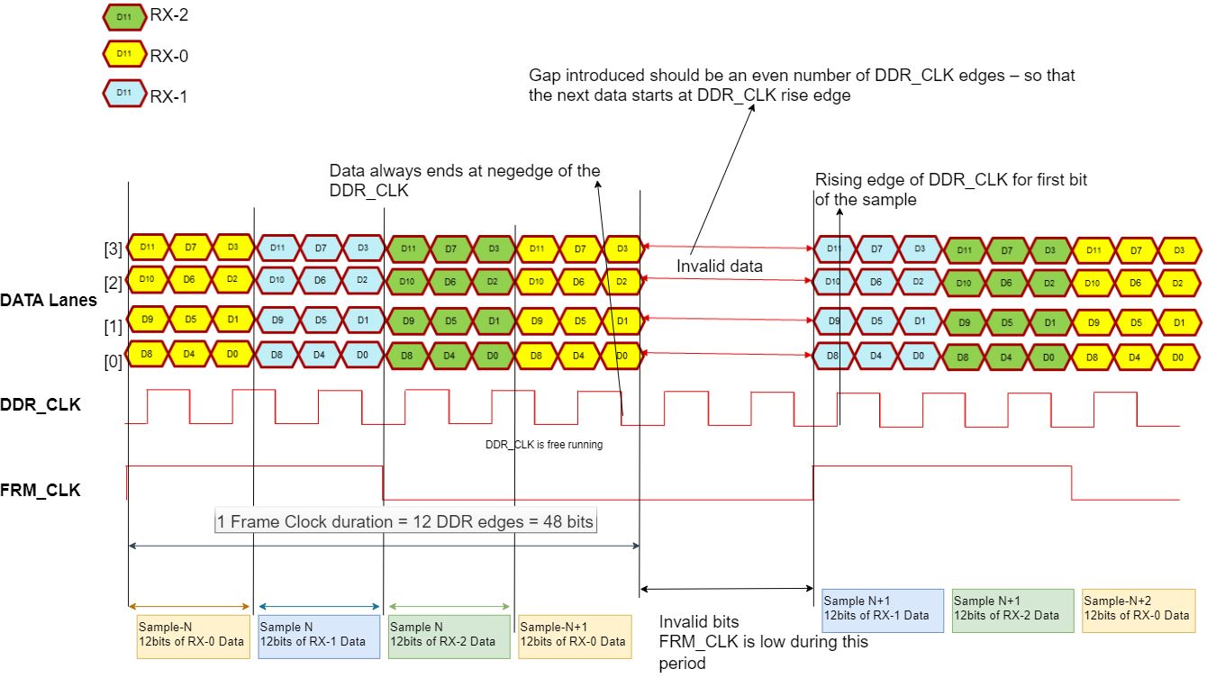
RDIF Data Format

AWRL1432 RDIF Data FormatFigure 7-16 RDIF Data Format

  • The samples are sent one channel by one channel as shown in the diagram above. All the 12-bits of one channel are sent on 4 data lanes in 3 DDR_CLK edges, followed by next RX channel.

  • The frame clock (FRM_CLK) spans 12 DDR_CLK edges and 48 bits are sent in 1 FRM_CLK

  • The FRM_CLK can have gaps in between. This is required as the interface rate is greater than the incoming rate

  • DDR_CLK is continuous.

  • DDR_CLK is generated from 400MHz ADC CLK (one of the ADC CLKs) - selected for the DFE. It is the same 400MHz clock selected for DFE.

  • New sample always starts at the rise edge of the DDR_CLK

  • The FRM_CLK is valid for the entire data bit and is meets the Tsu/Th wrt DDR_CLK.