SLUS784E December 2007 – December 2015
PRODUCTION DATA.
- 1 Features
- 2 Applications
- 3 Description
- 4 Revision History
- 5 Device Options
- 6 Pin Configuration and Functions
- 7 Specifications
-
8 Detailed Description
- 8.1 Overview
- 8.2 Functional Block Diagram
- 8.3
Feature Description
- 8.3.1 Control Logic Overview
- 8.3.2 Temperature Qualification (Applies Only to Versions With TS Pin Option)
- 8.3.3 Input Overvoltage Detection, Power Good Status Output
- 8.3.4 Charge Status Outputs
- 8.3.5 Battery Charging: Constant Current Phase
- 8.3.6 Charge Current Translator
- 8.3.7 Battery Voltage Regulation
- 8.3.8 Pre-Charge Timer
- 8.3.9 Thermal Protection Loop
- 8.3.10 Thermal Shutdown And Protection
- 8.3.11 Dynamic Timer Function
- 8.3.12 Charge Termination Detection and Recharge
- 8.3.13 Battery Absent Detection - Voltage Mode Algorithm
- 8.3.14 Charge Safety Timer
- 8.3.15 Short-Circuit Protection
- 8.3.16 Startup With Deeply Depleted Battery Connected
- 8.4 Device Functional Modes
- 9 Application and Implementation
- 10Power Supply Recommendations
- 11Layout
- 12Device and Documentation Support
- 13Mechanical, Packaging, and Orderable Information
Package Options
Refer to the PDF data sheet for device specific package drawings
Mechanical Data (Package|Pins)
- DRC|10
Thermal pad, mechanical data (Package|Pins)
- DRC|10
Orderable Information
9 Application and Implementation
NOTE
Information in the following applications sections is not part of the TI component specification, and TI does not warrant its accuracy or completeness. TI’s customers are responsible for determining suitability of components for their purposes. Customers should validate and test their design implementation to confirm system functionality.
9.1 Application Information
The bq24085/6/7/8 series are highly integrated Li-Ion and Li-Pol linear chargers, targeted at space-limited portable applications. The battery is charged in three phases: conditioning, constant or thermally regulated current, and constant voltage. An internal programmable charge timer provides a backup protection feature for charge termination and is dynamically adjusted during the thermal regulation phase.
9.2 Typical Applications
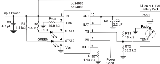
The typical application diagrams shown here are configured for 400 mA fast charge current, 40 mA pre-charge current, 5 hour safety timer and 30 min pre-charge timer.
9.2.1 bq24086 and bq24088 Typical Application
9.2.1.1 Design Requirements
9.2.1.2 Detailed Design Procedure
9.2.1.2.1 Selecting Input and Output Capacitor
In most applications, all that is needed is a high-frequency decoupling capacitor on the input power pin. A 1-μF ceramic capacitor, placed in close proximity to the IN pin and GND pad, works fine. In some applications, depending on the power supply characteristics and cable length, it may be necessary to increase the input filter capacitor to avoid exceeding the IN pin maximum voltage rating during adapter hot plug events.
The bq2408x, at low charge currents, requires a small output capacitor for loop stability. A 0.1-μF ceramic capacitor placed between the BAT and ISET pad is typically sufficient.
9.2.1.2.2 Using Adapters With Large Output Voltage Ripple
Some low cost adapters implement a half rectifier topology, which causes the adapter output voltage to fall below the battery voltage during part of the cycle. To enable operation with low cost adapters under those conditions the bq2408x family keeps the charger on for at least 25 msec (typical) after the input power puts the part in sleep mode. This feature enables use of external low cost adapters using 50-Hz networks.
The backgate control circuit prevents any reverse current flowing from the battery to the adapter terminal during the charger off delay time.
NOTE
The PG pin is not deglitched, and it indicates input power loss immediately after the input voltage falls below the output voltage. If the input source frequently drops below the output voltage and recovers, a small capacitor can be used from PG to VSS to prevent PG flashing events.
9.2.1.2.3 Calculations
Program the charge current for 400 mA:
where
- from the Electrical Characteristics table. . . V(SET) = 2.5 V
- from the Electrical Characteristics table. . . K(SET) = 182
Selecting the closest standard value, use a 1.13-kΩ resistor connected between ISET (pin 6) and ground.
Program 5-hour safety timer timeout:
where
- from the Electrical Characteristics table. . . K(CHG) = 0.1 hr / kΩ
Selecting the closest standard value, use a 49.9-kΩ resistor connected between TMR (pin 2) and ground.
Disable the temp sense function:
A constant voltage between VTS1 and VTS2 on the TS input disables the temp sense function.
from the Electrical Characteristics table. . . V(TS1) = 30% × VIN
from the Electrical Characteristics table. . . V(TS2) = 61% × VIN
A constant voltage of 50% × Vin disables the temp sense function, so a divide-by-2 resistor divider connected between Vin and ground can be used. Two 1-MΩ resistors keeps the power dissipated in this divider to a minimum.
For a 0 to 45°C range with a Semitec 103AT thermistor, the thermistor values are 4912 at 45°C and 27.28 k at 0°C. RT1 (top resistor) and RT2 (bottom resistor) are calculated in Equation 12:

| PIN | COMPONENTS |
| IN | In most applications, the minimum input capacitance needed is a 0.1-μF ceramic decoupling capacitor near the input pin connected to ground (preferably to a ground plane through vias). The recommended amount of input capacitance is 1 μF or at least as much as on the output pin. This added capacitance helps with hot plug transients, input inductance and initial charge transients. |
| OUT | There is no minimum value for capacitance for this output, but TI recommends to connect a 1-μF ceramic capacitor between OUT and ground. This capacitance helps with termination, and cycling frequency between charge done and refresh charge when no battery is present. It also helps cancel out any battery lead inductance for long leaded battery packs. TI also recommends to put as much ceramic capacitance on the input as the output so as not to cause a drop out of the input when charging is initiated. |
| ISET/BAT | For stability reasons, it may be necessary to put a 0.1-μF capacitor between the ISET and BAT pin.. |
| STAT1/2 and PG | Optional (LED STATUS – See below, Processor Monitored; or no status) |
| STAT1 | Connect the cathode of a red LED to the open-collector STAT1 output, and connect the anode of the red LED to the input supply through a 1.5-kΩ resistor that limits the current. |
| STAT2 | Connect the cathode of a green LED to the open-collector STAT2 output, and connect the anode of the green LED to the input supply through a 1.5-kΩ resistor that limits the current. |
| PG | Connect the cathode of an LED to the open-collector PG output, and connect the anode of the LED to the input supply through a 1.5-kΩ resistor to limit the current. |
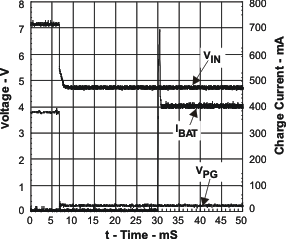
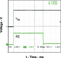
9.2.1.3 Application Curves
9.2.2 bq24085 Typical Application
Figure 21 illustrates the typical application circuit for bq24085.
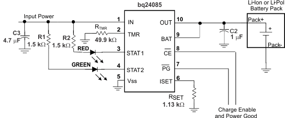 Figure 21. bq24085 Application Schematic
9.2.2.1 Design Requirements
Follow the design requirements in bq24086 and bq24088 Typical Application.
9.2.3 bq24087 Typical Application
Figure 22 shows the typical application circuit for bq24087.
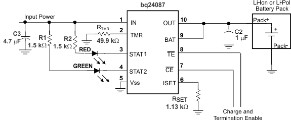 Figure 22. bq24087 Application Schematic
9.2.3.1 Design Requirements
Follow the design requirements in bq24086 and bq24088 Typical Application.
